Affiliated centres, institutes and facilities
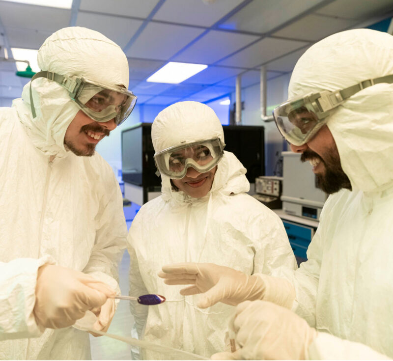
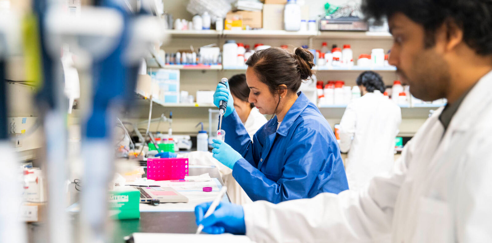
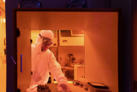
In the department of Engineering Physics, affiliated centres, institutes and facilities contribute to the overall academic environment by serving as spaces for conducting research, organizing activities and providing additional resources and cutting-edge equipment for students and faculty. These hubs are places for knowledge creation and application, emphasizing collaboration and shared goals.
-
Centre for Emerging Device Technologies (CEDT)
Learn moreThe CEDT is dedicated to research in optoelectronic and electronic devices. Research projects include molecular beam epitaxial deposition of semiconductor materials and structures for optoelectronic applications, and various processing technologies necessary for optoelectronic devices.
-
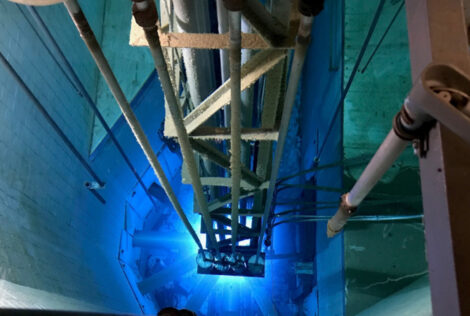
McMaster Nuclear Reactor
Visit website (Opens in new window)A 5 MW multi-purpose reactor that provides neutrons for research and medical isotope production. It is Canada’s most powerful research reactor and the nation’s only major neutron source.
The Canadian Centre for Electron Microscopy (CCEM) provides world-class electron microscopy capabilities and expertise to Canadian researchers and industry working in a broad range of fields. Our vision is to be one of the leading electron microscopy facilities in the world for the quality of the scientific research, to be the go-to provider of electron microscopy services to Canadian industry and to play a leading role in promoting interactions amongst researchers in various fields nationally and internationally.
Director(s)
Dr. Nabil Bassim
Professor
bassimn@mcmaster.ca
905-525-9140 ext. 24102
A state-of-the-art light microscopy facility with a mandate to support high quality scientific research, promote cross-disciplinary interactions among researchers in science, engineering and life sciences, and train future generations of microscropists.
The Biointerfaces Institute is a state-of-the-art facility implementing high-throughput research pipelines to investigate the nature of the biological/material interface, or biointerface.
The Brockhouse Institute for Materials Research is an interdisciplinary research organization with the mandate to develop, support and co-ordinate all materials research-related activities at McMaster. The facilities of the Institute and its pool of expertise are also available to industry and organizations that require assistance with materials research and development or material analysis.