Access the CEDT
Safety training, booking equipment and training sessions, and qualifications form
The CEDT team operates and manages equipment under three facilities:

Use of equipment requires direct training from the CEDT. For certification or inquiries, please contact Doris Stevanovic or Nebile Isik Goktas.
| Atomic Layer Deposition System (PEALD) Arradiance GEMStar XT-DP 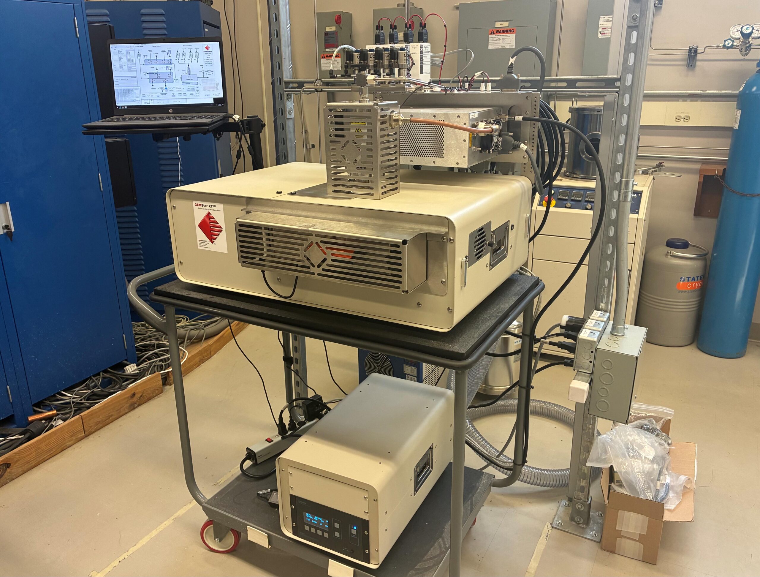 | Benchtop plasma-enhanced atomic layer deposition (PEALD) system for ultrathin conformal film growth and surface engineering applications. Supports conformal dielectric thin-film deposition including SiO2 and Al2O3 using plasma-assisted processing, pulsed precursor delivery, and mass flow-controlled gas handling. Location: TAB-110 Contact: Nebile Isik Goktas More details |
Critical Point Dryer Tousimis Autosamdri-815 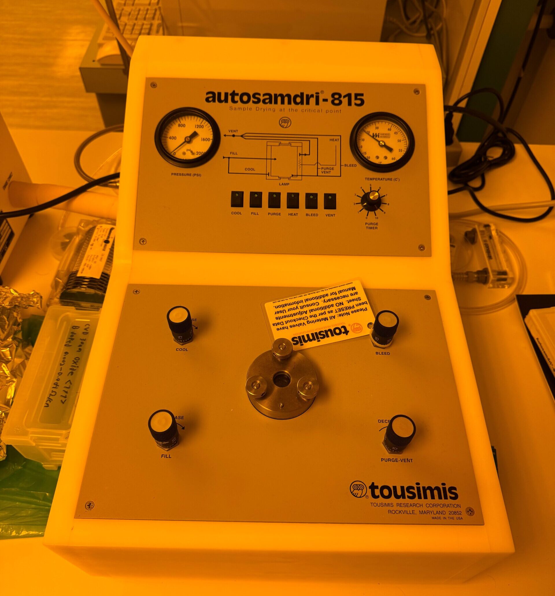 | Automatic supercritical point dryer for drying micro-electromechanical systems (MEMS) devices and small substrates using CO2 and liquid solvent exchange. Location: JHE–A306 Contact: Nebile Isik Goktas or Doris Stevanovic More details |
| Dicing Saw Disco DAD3221 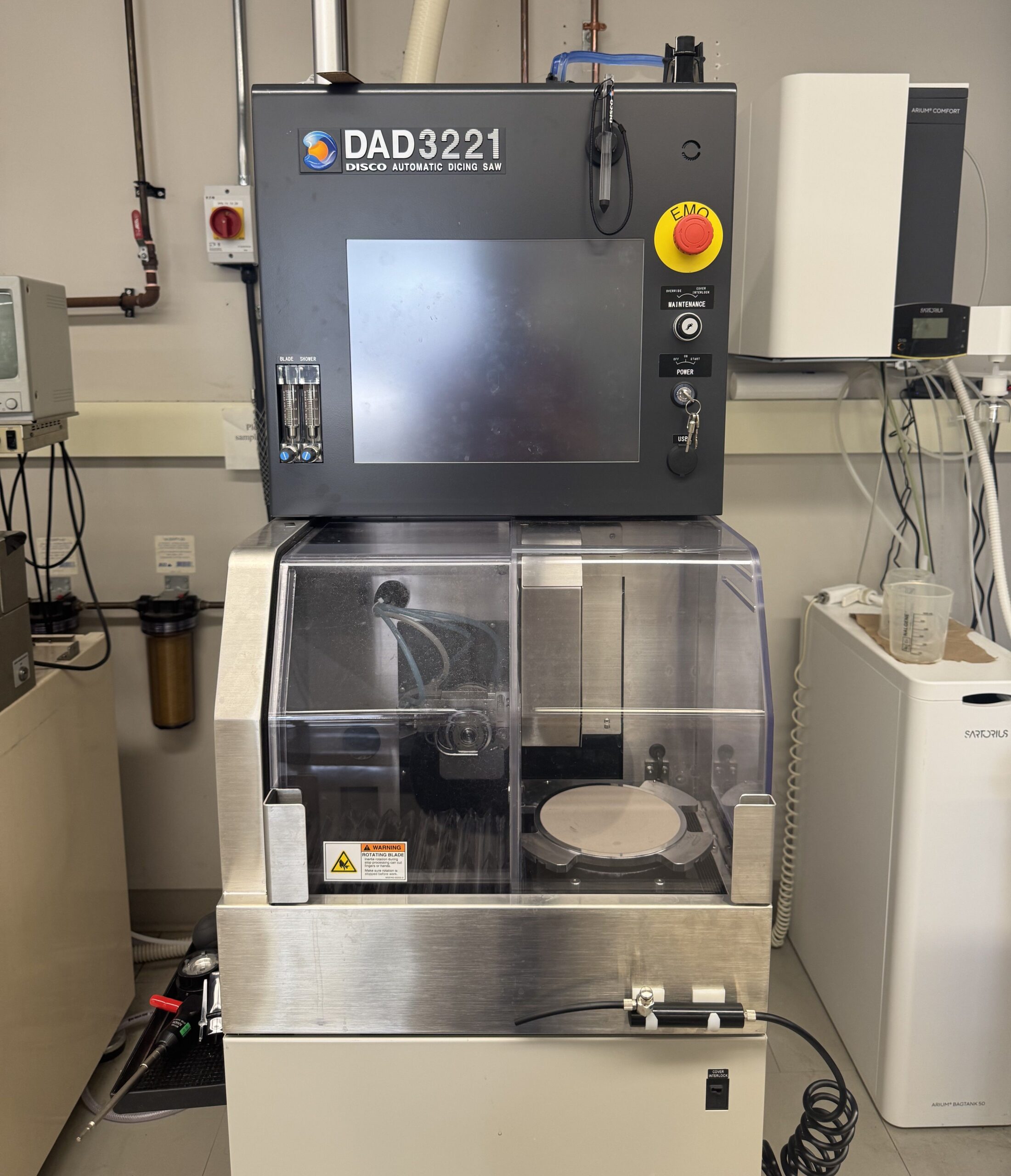 | Precision semiconductor dicing saw for cutting wafers, dies, and brittle substrates including semiconductor materials, glass, and ceramics. Supports manual operation or fully automated alignment and cutting workflows using integrated image-processing software. Location: TAB–205 Contact: Nebile Isik Goktas More details |
| E-Beam Evaporator [Custom-Made] 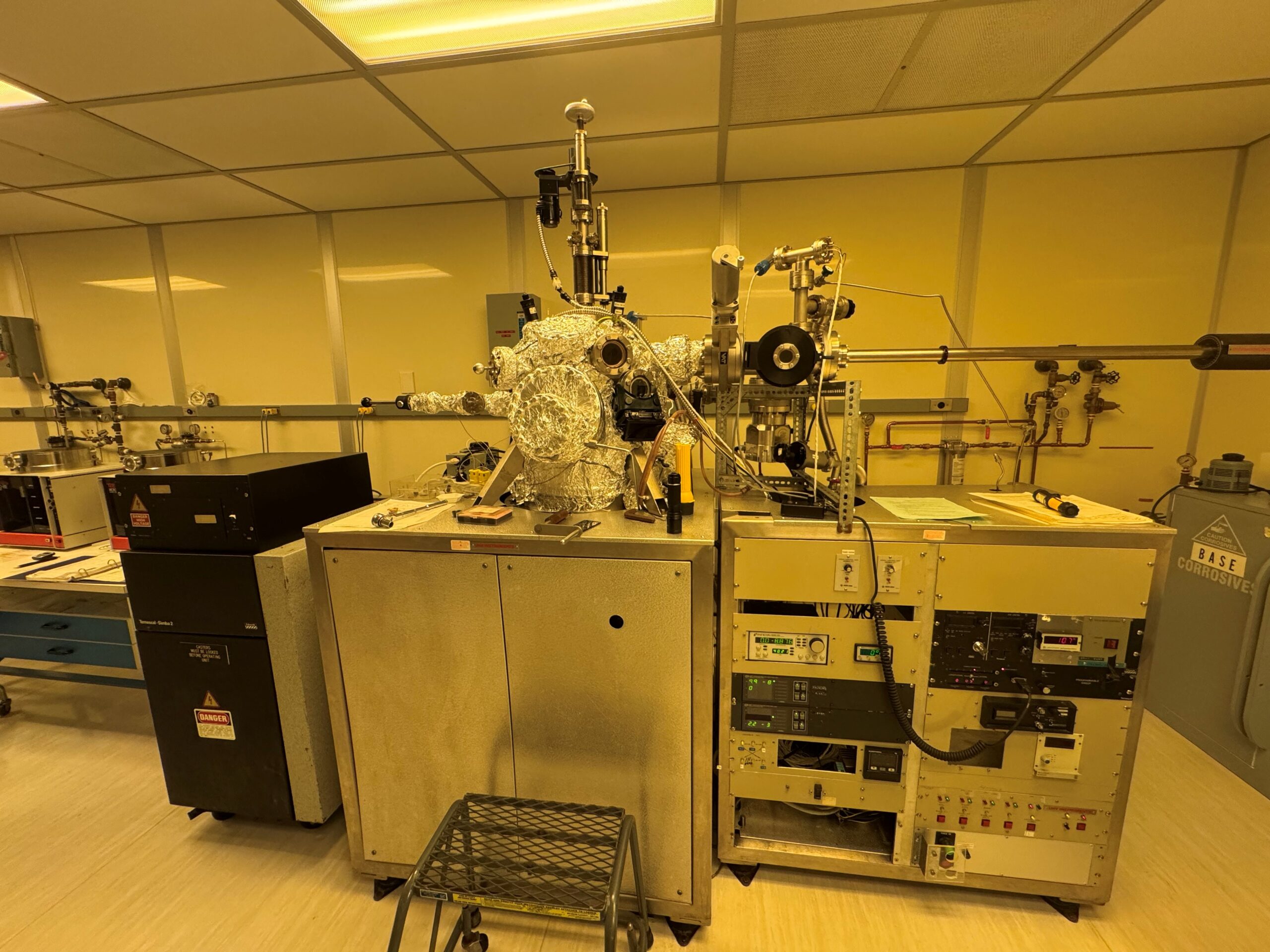 | E-beam deposition system for thin films under ultra-high vacuum (UHV) with load lock (10E-8 Torr). Capable of rotating and tilting samples. Compatible metals: Ni, Ge, Au, Ti, Pt, Cr with up to 3” diameter targets. Location: JHE-A306 Contact: Doris Stevanovic Details |
| Femtosecond Laser Manufacturing System FEMTIKA  | Hybrid femtosecond laser microfabrication platform supporting multiphoton polymerization, selective laser etching, and laser ablation processes. Integrates automatic beam alignment, real-time optical monitoring, vibration isolation, and nanoscale positioning for high-precision additive and subtractive manufacturing of polymeric, glass, and crystalline materials. Location: TAB-110 Contact: Nebile Isik Goktas More details |
| Fiber Optic Illuminator Dolan-Jenner Fiber-Lite 190  | High-intensity quartz halogen light source with flexible gooseneck fibre optic guide. Convection-cooled mechanism eliminates air particle generation, acoustic noise, and physical micro-vibrations. Location: JHE-A306 Contact: Nebile Isik Goktas or Doris Stevanovic Details |
| FT-IR Spectrometer – Vacuum Bruker Vertex 80V 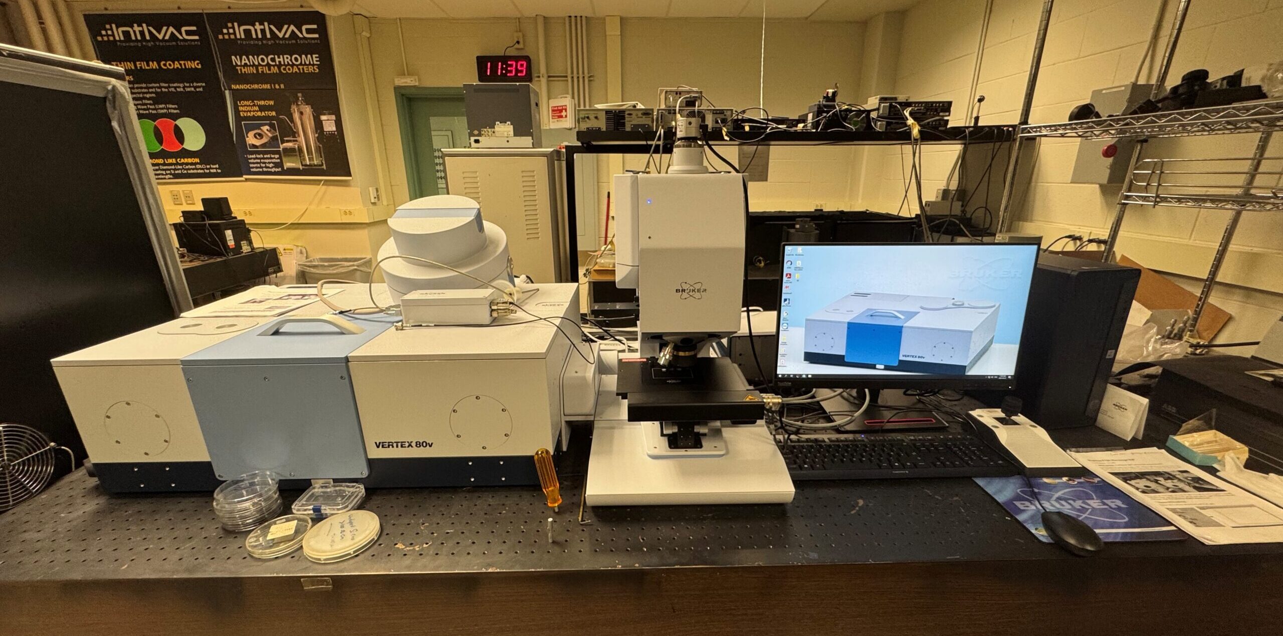 | High-resolution vacuum Fourier-transform infrared (FT-IR) spectrometer for molecular and thin-film spectral characterization across the UV to terahertz bands. Location: JHE-317 Contact: Nebile Isik Goktas More details |
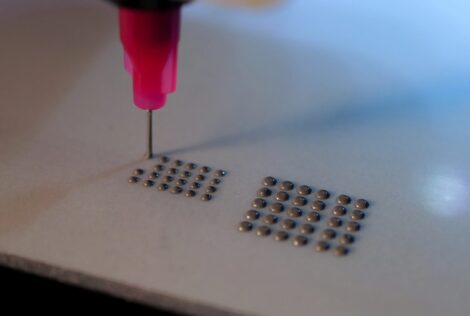
| Fluid Dispensing System – Non-Contact SonoPlot Microplotter II 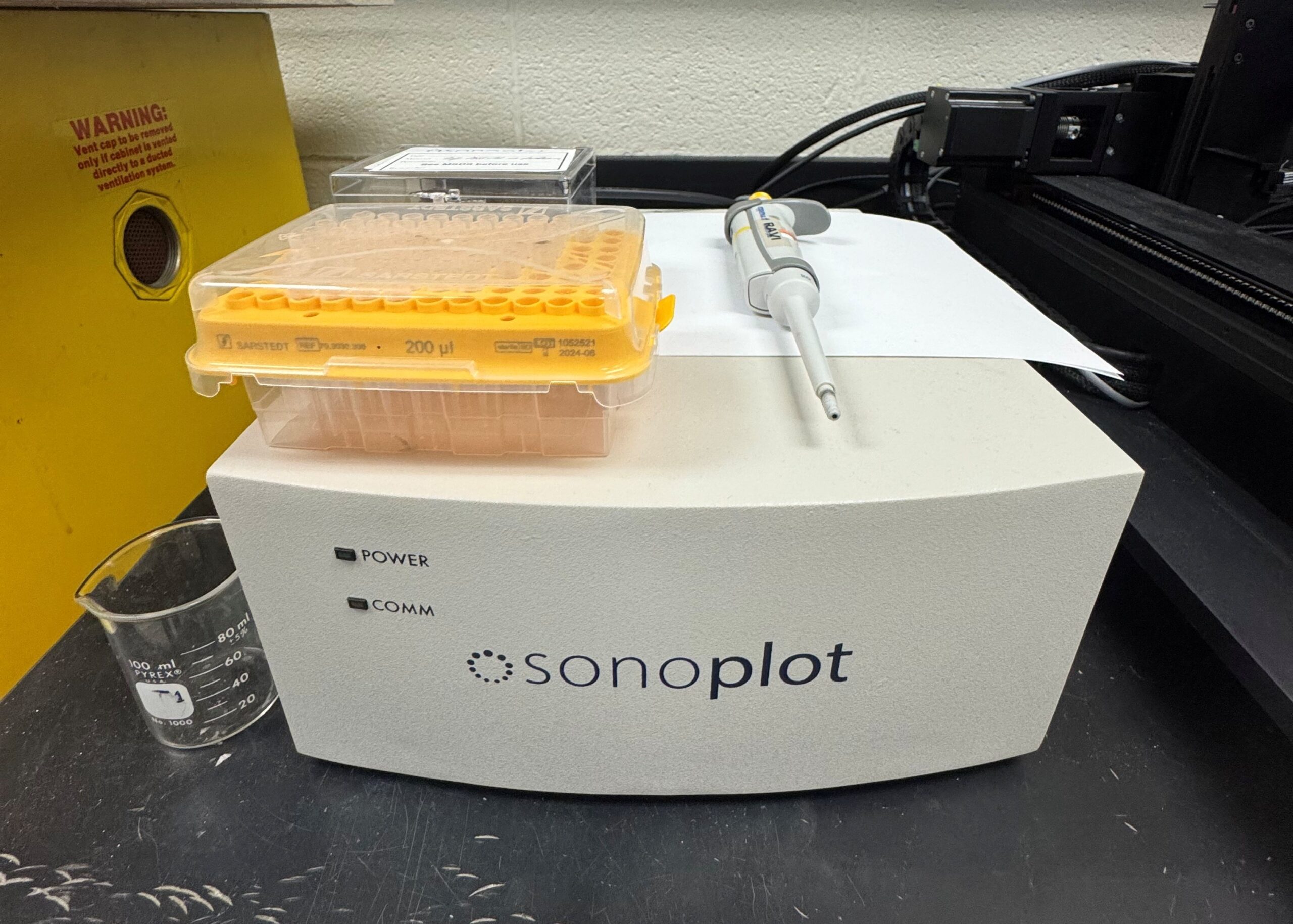 | Ultrasonic picoliter dispensing system for non-contact micro-patterning of functional inks and biological payloads. It automates surface tilt mapping to print custom patterns while tracking the process via an integrated CCD camera. Location: JHE-A305 Contact: Nebile Isik Goktas More details |
| Fume Hood TXH-5  | Total exhaust 5 ft wide laminar flow hood providing ISO Class 5 (formerly Class 100) cleanliness conditions via a self-contained HEPA fan filter module. Features a vertical-rising face shield and sealed LED light fixture. 2 in Cleanroom, 3 in Organic Lab. Location: TAB-205 Contact: Nebile Isik Goktas or Doris Stevanovic Details |
| Hall Effect Measurement System Nanometrics HL5500PC  | Turnkey Hall effect characterization system for electrical measurement of semiconductor materials, including sheet resistivity, carrier concentration, and carrier mobility across a broad resistivity and temperature range. Location: TAB-110 Contact: Nebile Isik Goktas More details |
| Ion Implanter Whickham M50 Series  | Ion implantation system capable of generating, mass-selecting, and accelerating a broad range of ion species for semiconductor doping and materials modification applications. Location: TAB-110 Contact: Doris Stevanovic More details |
| Laminar Flow Cabinet – Locally Exhausted Canadian Cabinets  | Total exhaust 5 ft wide laminar flow hood providing ISO Class 5 (formerly Class 100) cleanliness conditions via a self-contained HEPA fan filter module. Features a vertical-rising face shield and sealed LED light fixture. 1 in Cleanroom (for etching and cleaning), 1 in Compound Semiconductor Lab (for polishing). Location: JHE-A306 Contact: Nebile Isik Goktas or Doris Stevanovic Details |
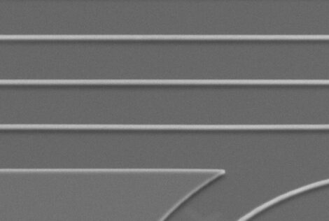
| Laser Lithography System Heidelberg μPG 101 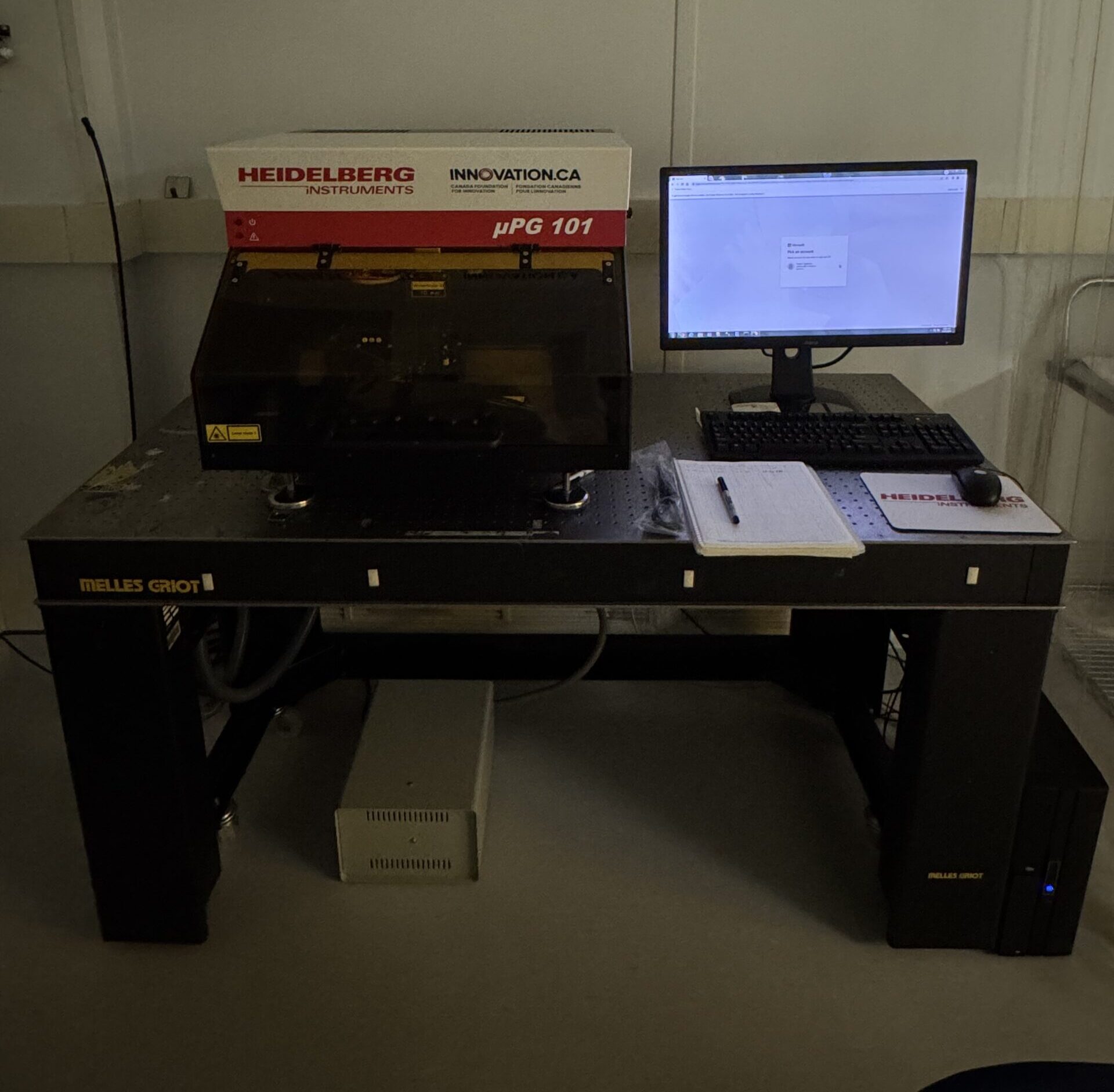 | Micro-pattern generator for direct writing applications and low-volume mask making. Supports grayscale lithography, manual alignment via an integrated camera system, and in situ design previewing using Exposure Wizard software. Location: JHE-A306 Contact: Nebile Isik Goktas More details |
| Mask Aligner Karl Suss MJB3 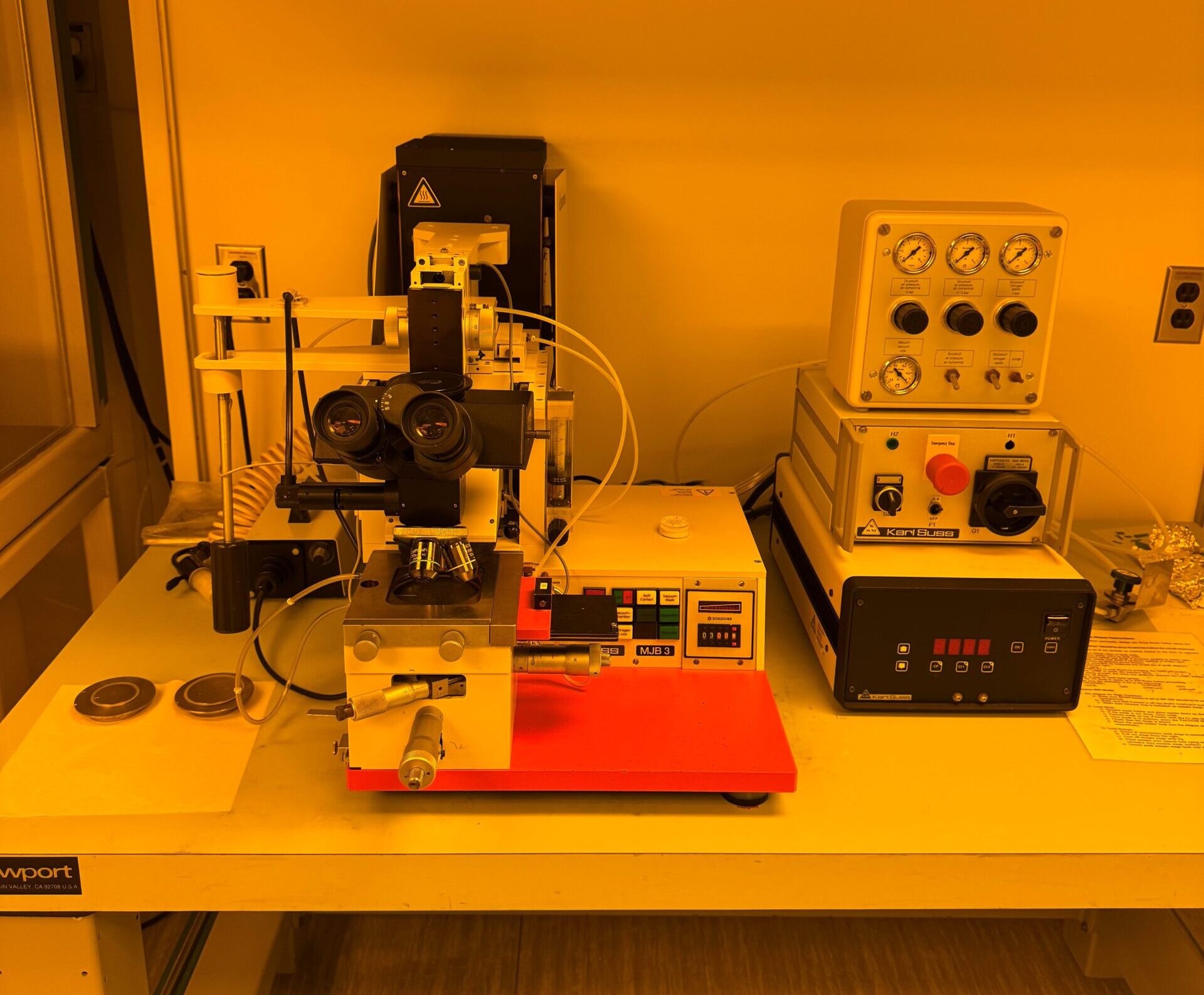 | Mask aligner for high-resolution UV photolithography and wafer alignment. Provides exposure options in vacuum contact, hard contact, soft contact, or proximity modes. Location: JHE-A306 Contact: Doris Stevanovic More details |
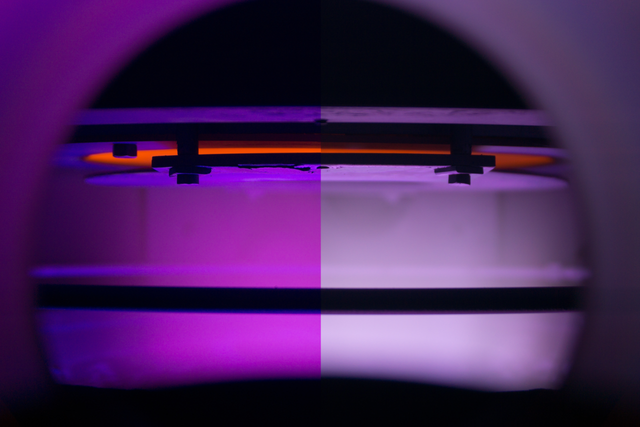
| Metal Organic Chemical Vapour Deposition System SMI EPIC MOCVD  | Metal organic chemical vapour deposition (MOCVD) system for epitaxial growth of high-purity crystalline compound semiconductor thin films. Utilizes hydrogen-rich processing environments, independently controlled heating zones, and precision gas flow control for advanced III-V semiconductor growth. Location: TAB-205 Contact: Nebile Isik Goktas or Doris Stevanovic More details |
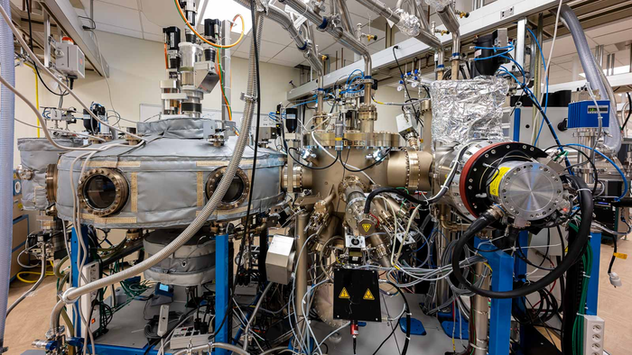
| Molecular Beam Epitaxy System – Gas Source MBE SVT Associates 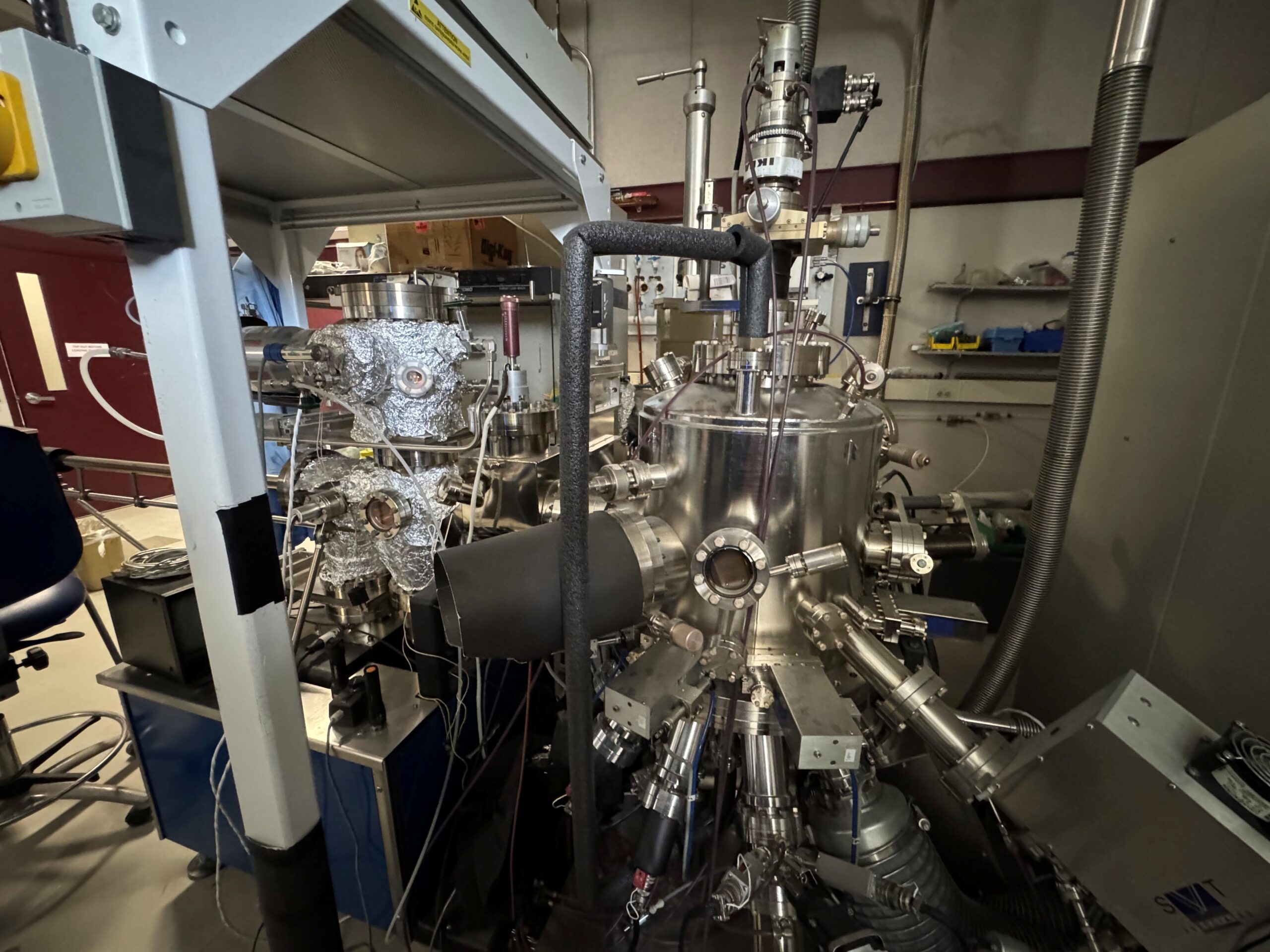 | Ultra-high vacuum molecular beam epitaxy (MBE) system utilizing thermally cracked gas precursors and solid evaporation sources for epitaxial growth of high-purity semiconductor thin films with atomic-scale thickness control. Location: TAB-110 Contact: Nebile Isik Goktas More details |
| Optical Microscope Leica DMR 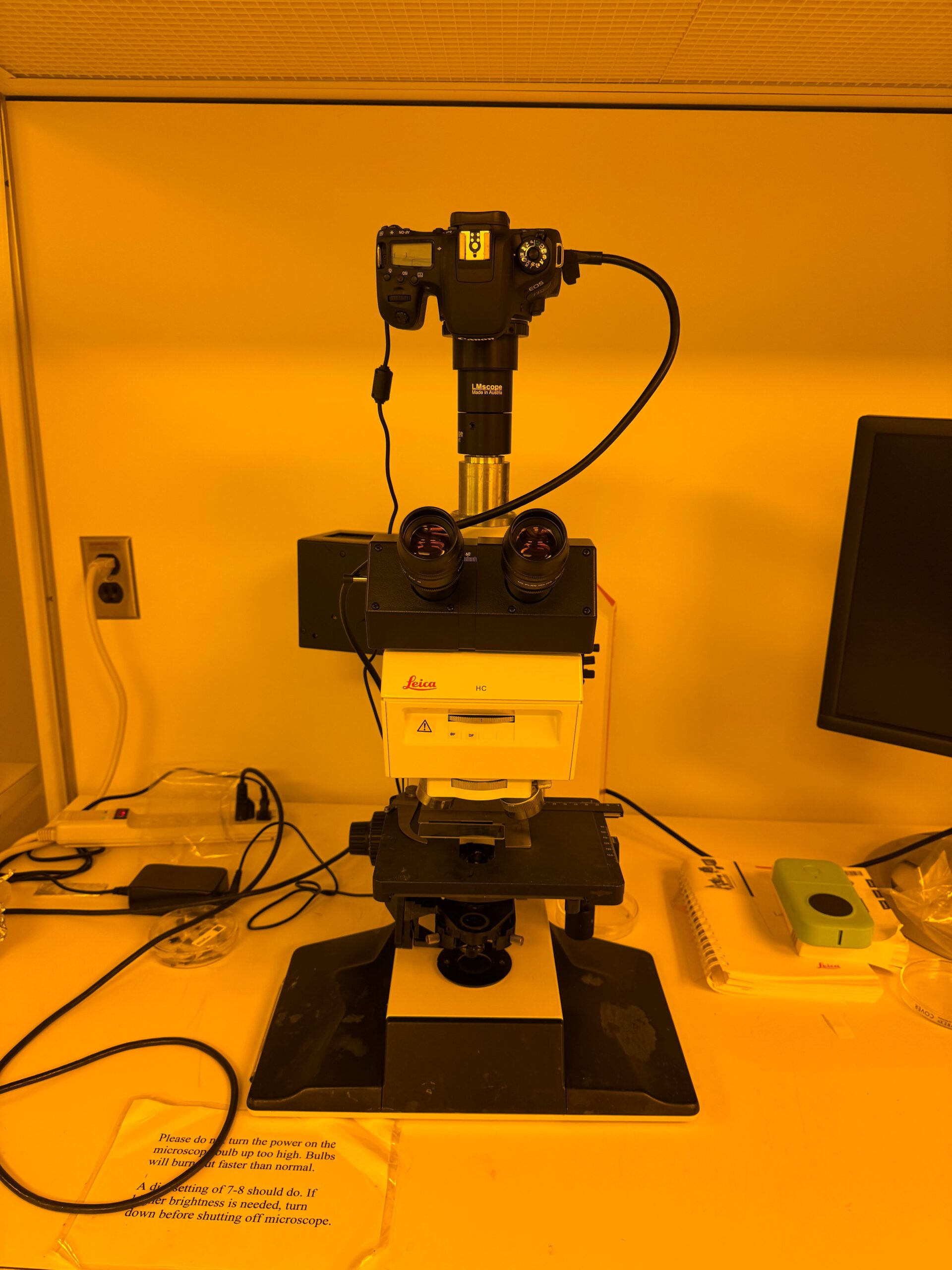 | Wide-field white-light LED illumination with objective lens up to 100x magnification. Equipped with 24 megapixel Canon 77D camera. Location: JHE-A306 Contact: Nebile Isik Goktas or Doris Stevanovic Details |
| Optical Polishing System KrellTech NOVA 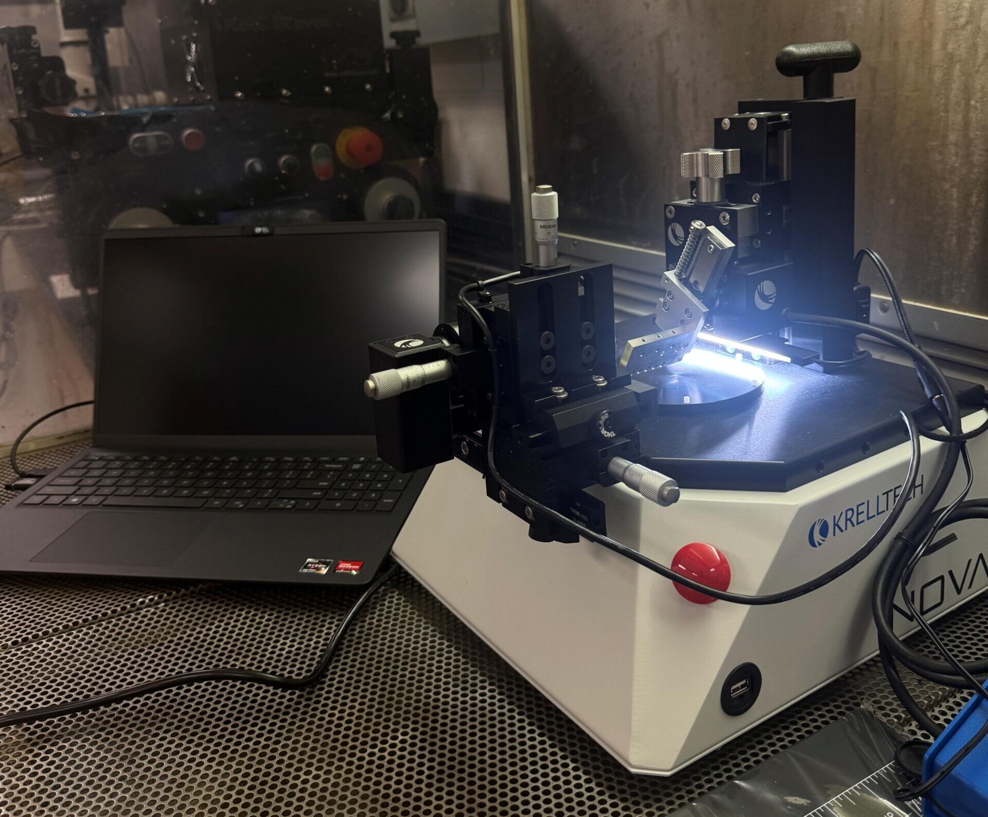 | Automated platform for precision optical surface polishing. Suitable for fiber optic connectors and bare fibers, photonic integrated circuits (PICs), waveguides, and custom optical component. Location: JHE-A305 Contact: Nebile Isik Goktas More details |
| Optical Table Newport RS2000 UCS 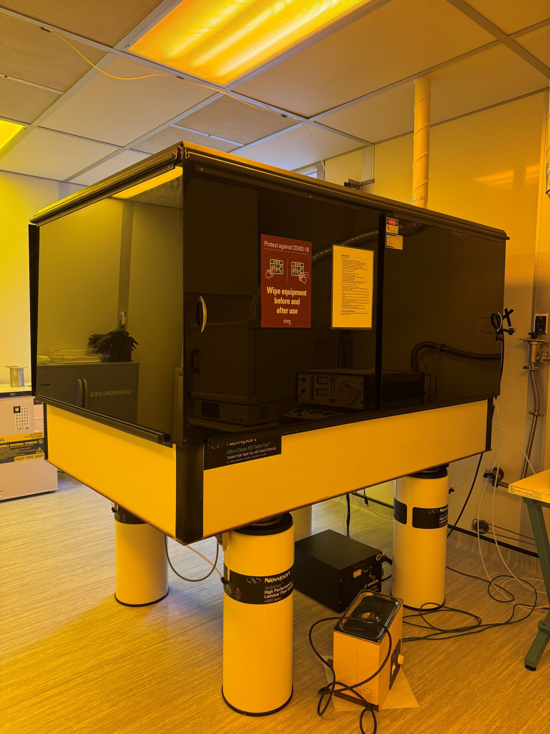 | Broadband damped optical tabletop engineered for vibration-sensitive optical and imaging experiments. Incorporates three tuned mass dampers, a constrained-layer damping core, and a damped ferromagnetic stainless steel work surface. 1 in Cleanroom, 1 in Characterization Lab. Location: JHE-A306 Contact: Nebile Isik Goktas or Doris Stevanovic More details |
| Parylene Coating System Specialty Coating Systems Labcoter® 2 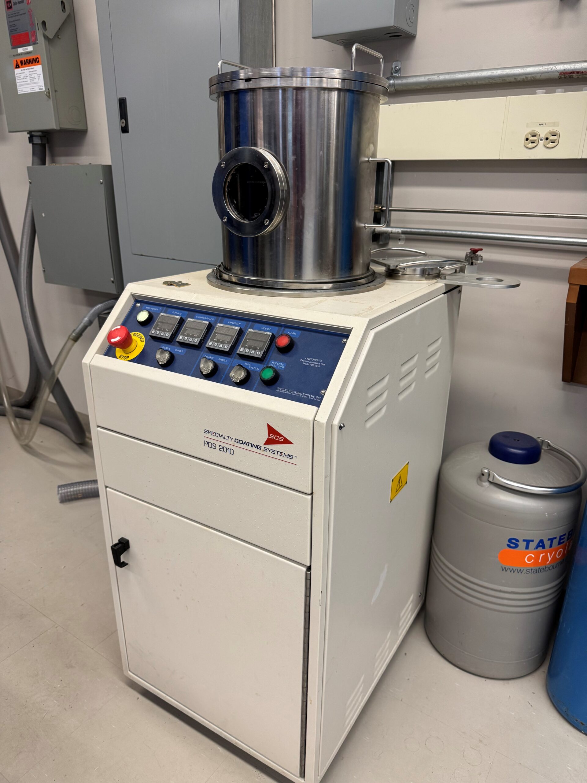 | Conformal parylene coating deposition system designed for uniform polymer encapsulation and surface protection of electronic, biomedical, and MEMS devices. Location: TAB-110 Contact: Nebile Isik Goktas or Doris Stevanovic More details |
| PECVD Thin Film Deposition System Technics Micro-PD Series 900 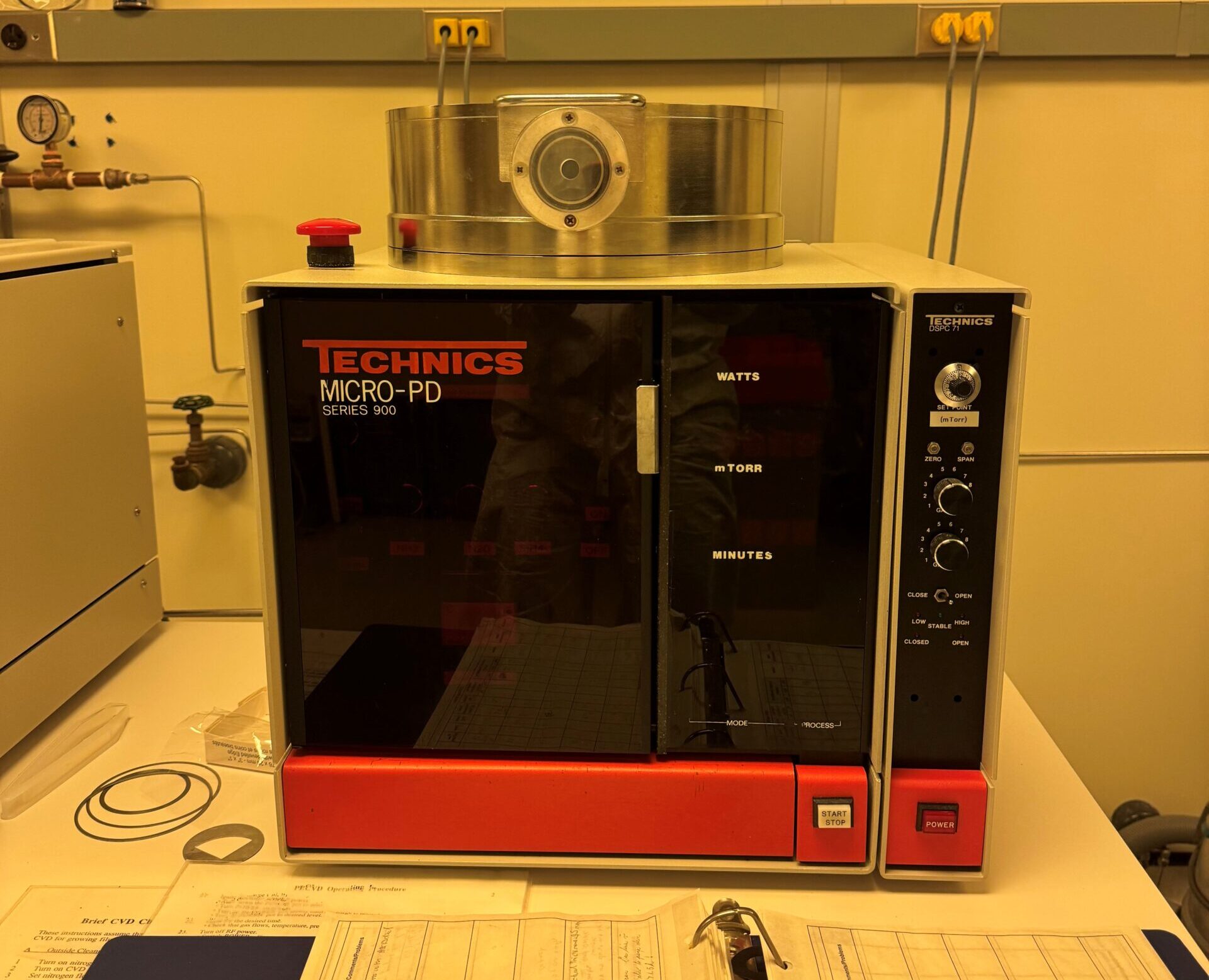 | Plasma-enhanced chemical vapour deposition (PECVD) system for depositing silicon nitride, silicon dioxide, and amorphous silicon thin films. Features automated recipe execution and supports up to five independent gas inputs across a variety of substrate materials. Location: JHE-A306 Contact: Nebile Isik Goktas More details |
Photoluminescence System | Set-up for room-temperature photoluminescence (RTPL) used for characterization of silicon-based thin films. Equipped with Coherent OBIS 375 nm He-Cd diode laser with max power of 50 mW, Ocean Optics USB2000+ charge-couple device (CCD) spectrometer, mirror, sample holder, filter, analog/digital converter, and computer. Location: JHE-A317 Contact: Nebile Isik Goktas or Doris Stevanovic More details |
| Plasma Etcher – ICP-RIE Oxford PlasmaPro 100 Cobra 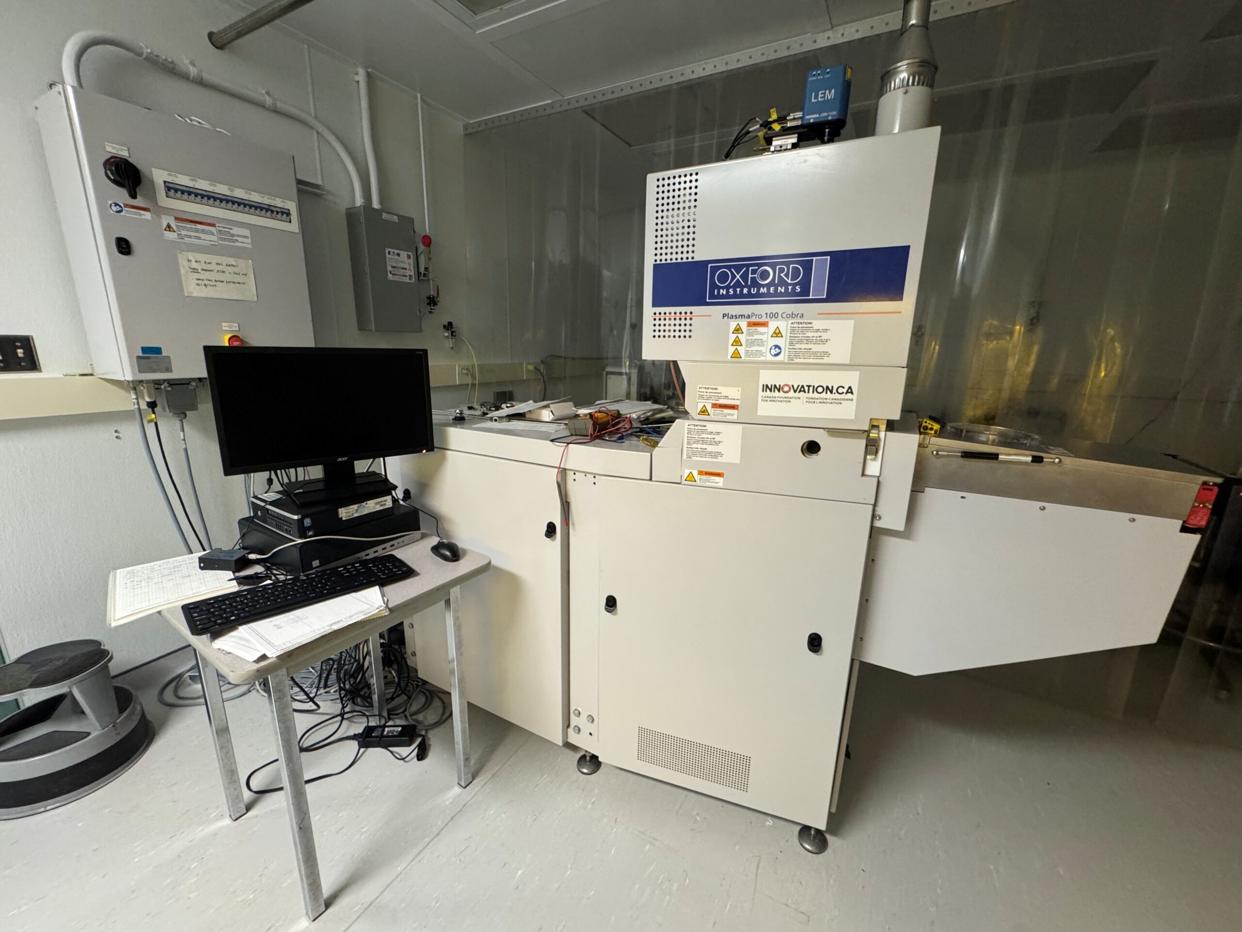 | High-density inductively coupled plasma reactive ion etching (ICP-RIE) system for dry etching. Supports independent ion energy control, helium backside cooling, and dual endpoint detection via optical emission spectroscopy and laser interferometry. Location: JHE-A306 Contact: Nebile Isik Goktas or Doris Stevanovic More details |
| Plasma Etcher – RIE Technics Micro-RIE Series 800  | Reactive ion etching (RIE) system designed for thin-film removal and ashing. Features three mass flow controlled gas channels and a water-cooled electrode process chamber designed to prevent cross-contamination. Location: JHE-A306 Contact: Nebile Isik Goktas More details |
| Rapid Thermal Annealing System – III-V JIPELEC JETFIRST 100 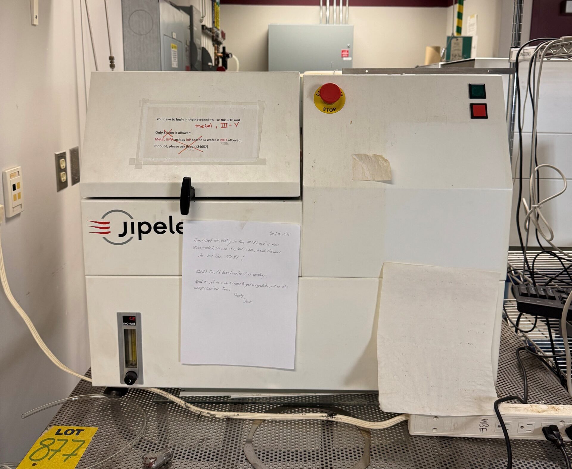 | Benchtop rapid thermal processing (RTP) system utilizing a cold-wall process chamber and multizone halogen lamp furnace for rapid thermal annealing of III-V semiconductor substrates. Integrated PIMS PC control software provides process monitoring, data acquisition, and pyrometer calibration across a broad temperature range. Location: TAB-205 Contact: Nebile Isik Goktas More details |
| Rapid Thermal Annealing System – III-V JIPELEC JETFIRST 100 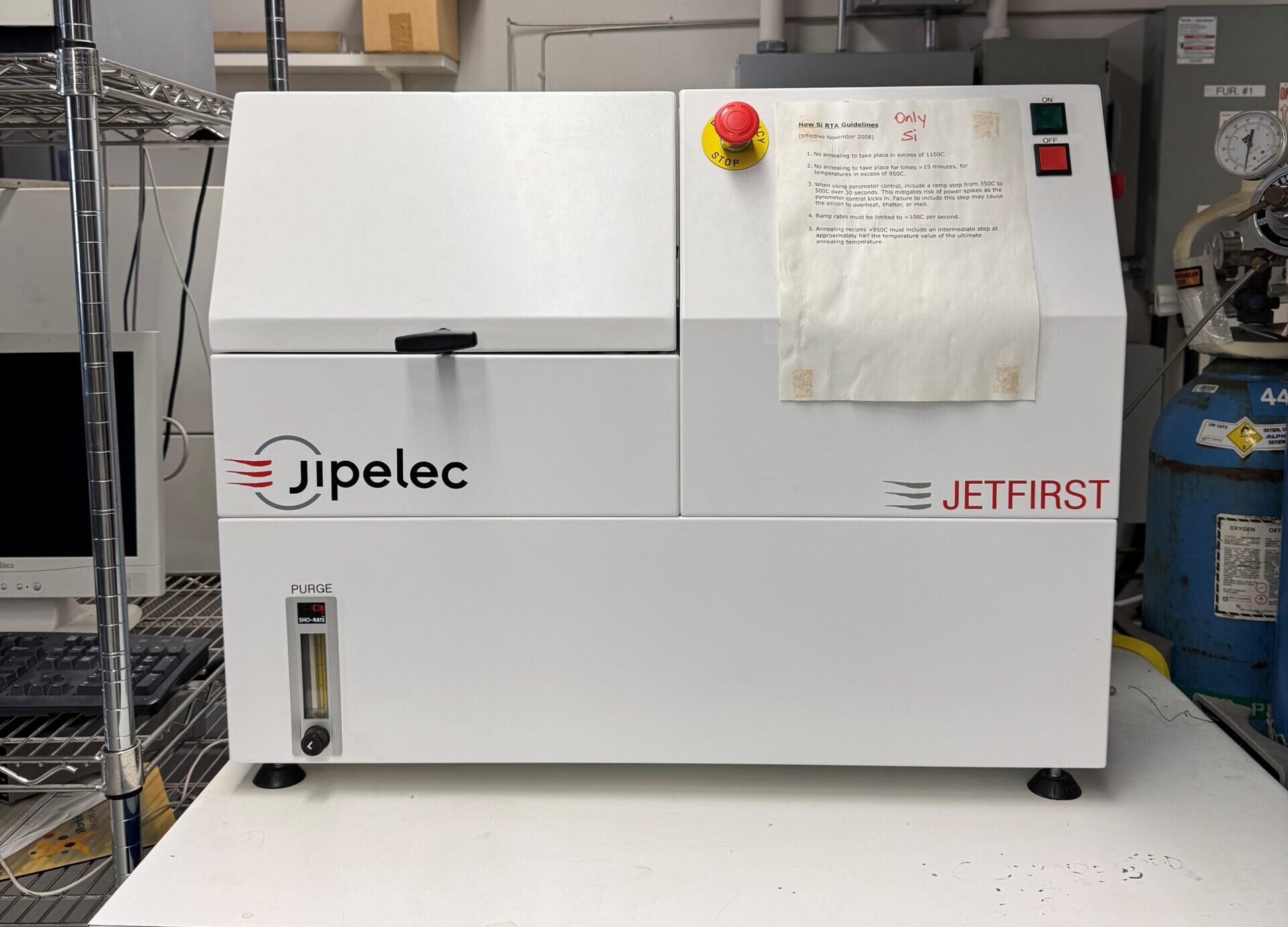 | Benchtop rapid thermal processing (RTP) system utilizing a cold-wall process chamber and multizone halogen lamp furnace for rapid thermal annealing of silicon-based semiconductor substrates. Integrated PIMS PC control software supports thermal process monitoring, data acquisition, and pyrometer calibration. Location: TAB-205 Contact: Nebile Isik Goktas More details |
| Roll-to-Roll Magnetron Sputtering System Angstrom Engineering 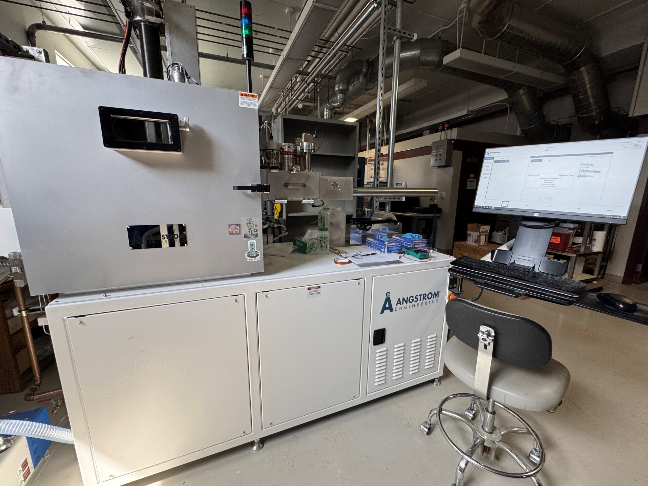 | Custom roll-to-roll magnetron sputtering platform designed for continuous deposition of uniform thin films onto flexible substrates. Supports reactive sputtering, RF substrate biasing, automated process recipes, and in situ optical monitoring for precision thin-film engineering. Location: TAB-110 Contact: Nebile Isik Goktas More details |
| Roll-to-Roll Slot-Die Coater infinityPV LR2RC 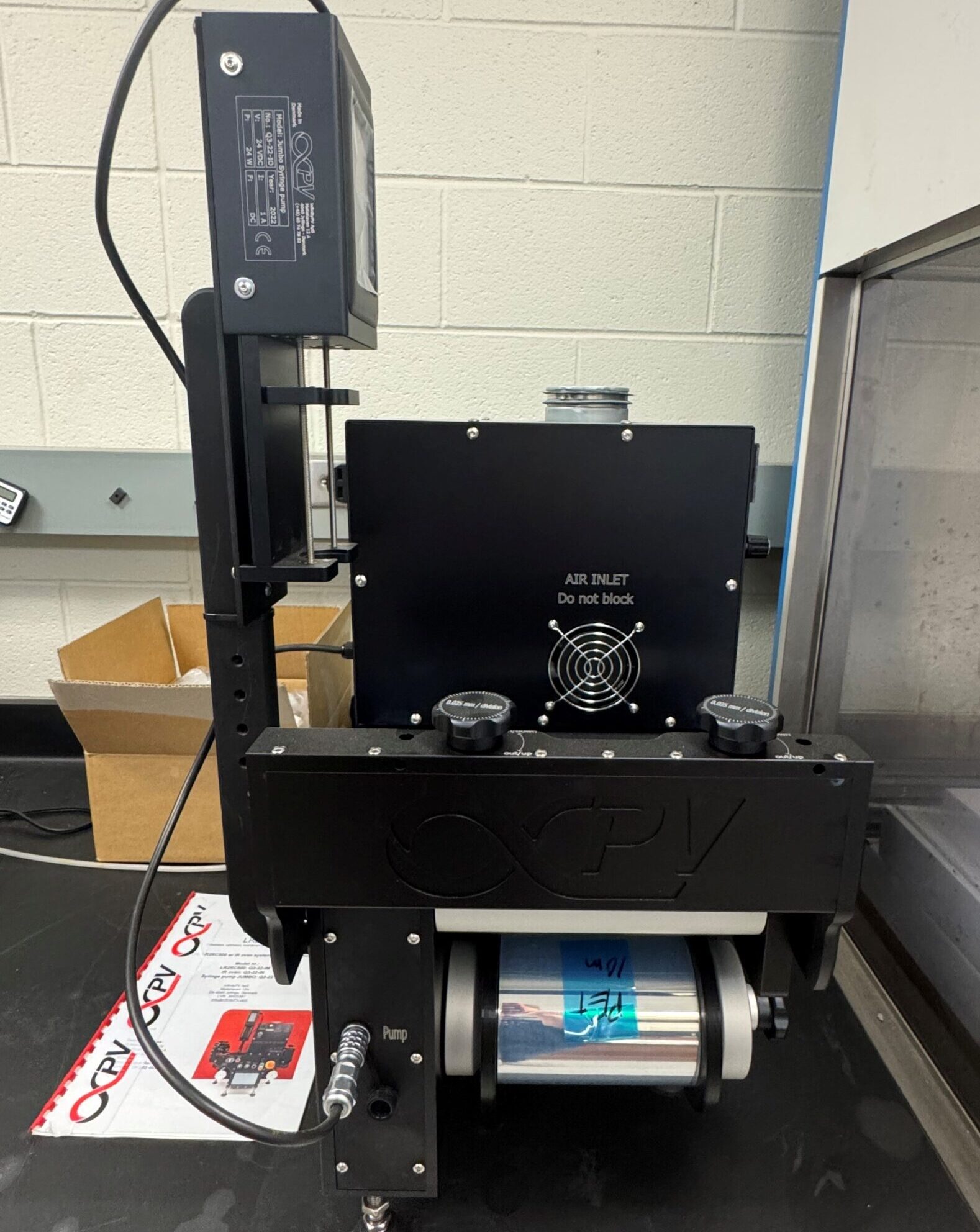 | Compact modular roll-to-roll slot-die coating platform designed for precision deposition and pilot-scale processing of functional thin films on flexible substrates. Supports continuous web handling, integrated drying/curing, and scalable process development for printed electronics and energy devices. Location: JHE-A305 Contact: Nebile Isik Goktas or Doris Stevanovic More details |
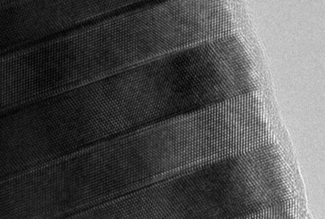
| Scanning Electron Microscope (SEM) – Benchtop JEOL JCM-6000 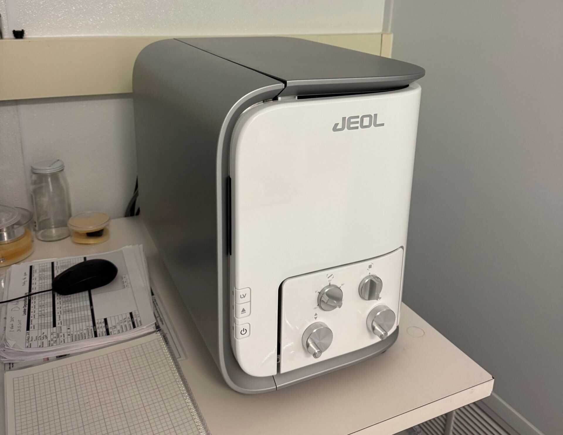 | Benchtop scanning electron microscope with secondary electron imaging (SEI) and backscattered electron (BSE) imaging capabilities. Includes an integrated JEOL energy dispersive spectrometer (EDS) for elemental point, line, and mapping analysis under high and low vacuum modes. Location: JHE-A306 Contact: Nebile Isik Goktas More details |
| Spectroscopic Ellipsometer – Variable Angle J.A. Woollam IR-VASE 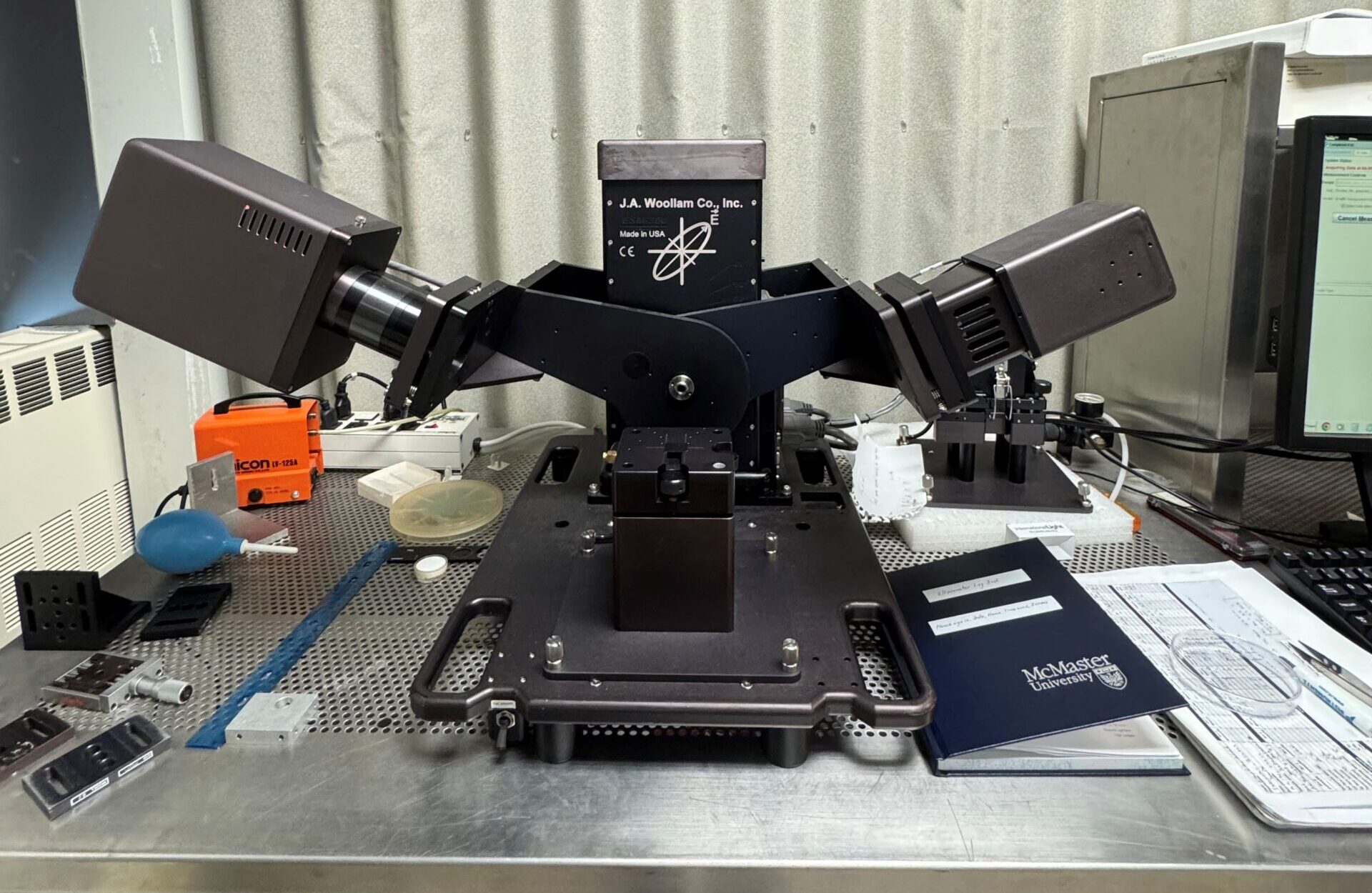 | Variable-angle spectroscopic ellipsometer for characterization of thin-film optical properties including thickness, refractive index, and extinction coefficient across ultraviolet, visible, and near-infrared wavelengths Location: JHE-317 Contact: Nebile Isik Goktas or Doris Stevanovic More details |
| Spin Coater WS-650 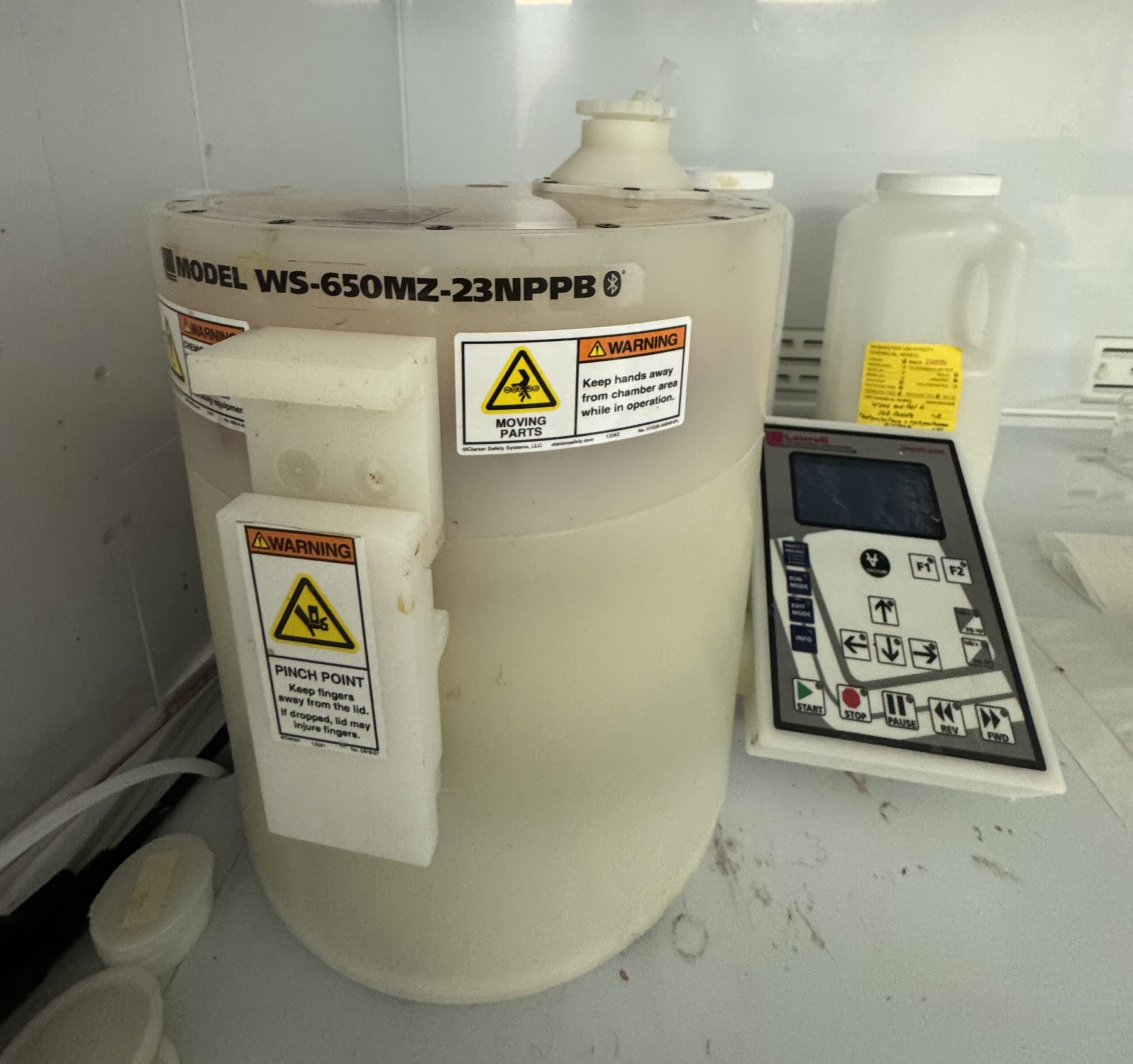 | Extremely precise rotation spinner with fully optimized process chamber and 7 programmable “recipes”. Accommodates up to 3” diameter wafers with max speed of 12,000 rpm (based on 100 mm silicon wafer). Location: JHE-A306 Contact: Nebile Isik Goktas or Doris Stevanovic Details |
| Spray Coater – Ultrasonic Sono-Tek Exacta-Coat 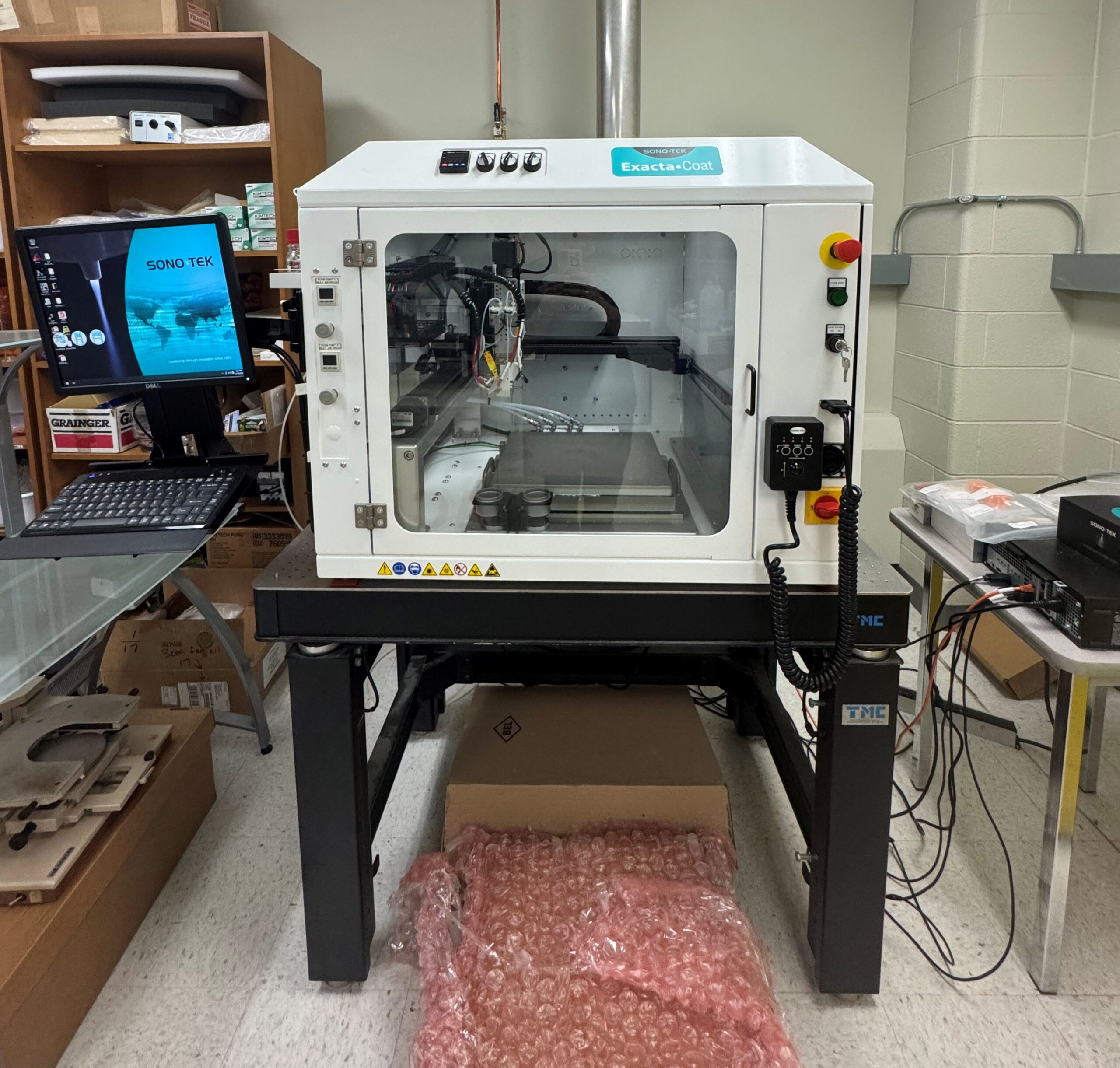 | Automated, programmable benchtop coating system for thin-film substrate processing, material development, and low-volume production. It utilizes a non-clogging ultrasonic spray nozzle with precision three-axis servo control to deposit uniform layers without shear-induced material breakdown. Location: JHE-A305 Contact: Nebile Isik Goktas More details |
| Sputter Deposition System Lesker PD500X3 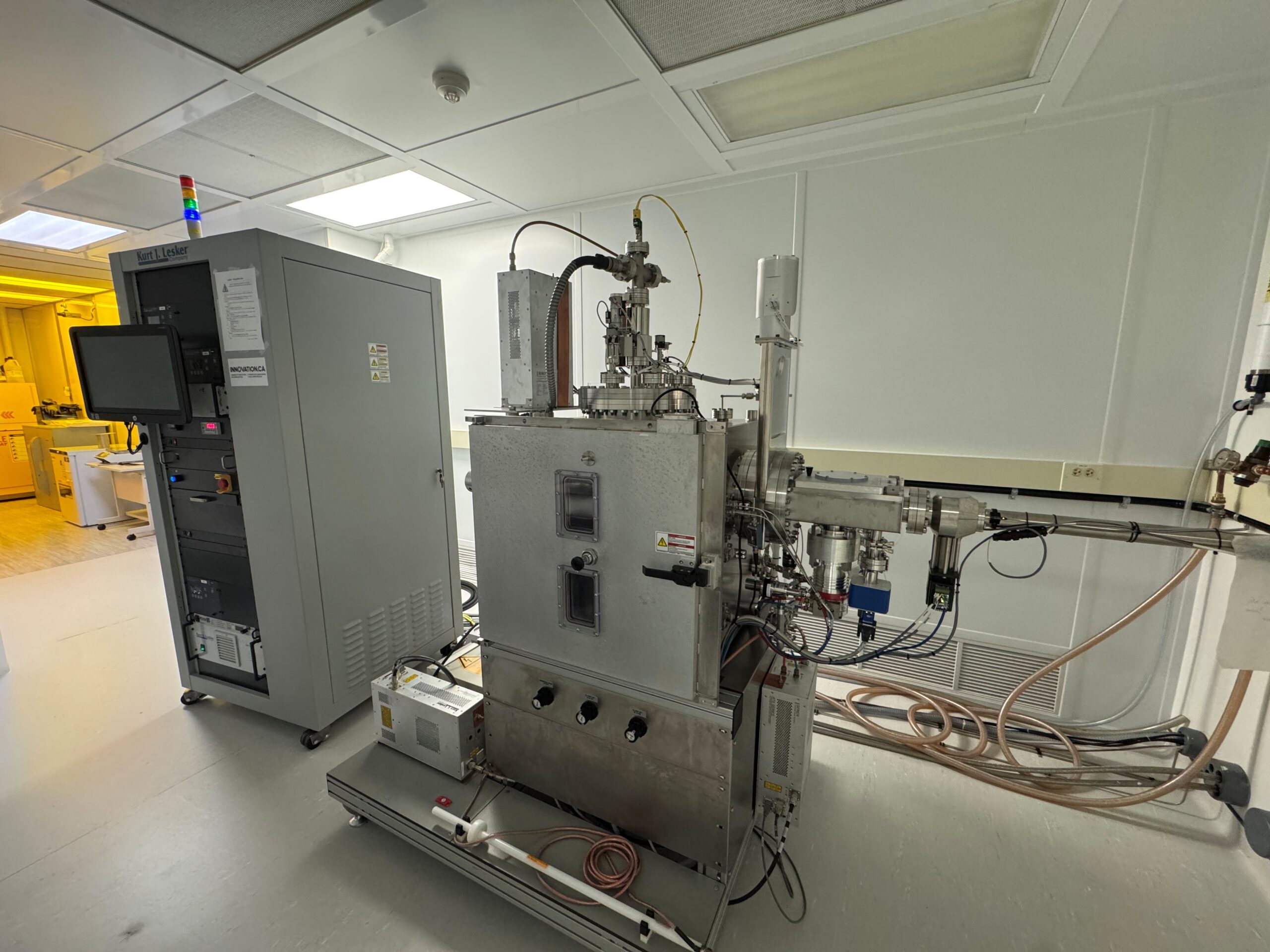 | Magnetron sputtering system designed for the deposition of dielectric and metal thin films. Utilizes an ultra-high vacuum (UHV) process chamber with a confocal source arrangement, computer-controlled processing software, and hardware configurations supporting the co-deposition of compound and doped films. Location: JHE-A306 Contact: Nebile Isik Goktas or Doris Stevanovic More details |
| Sputter Deposition System – Compact Research Coater Torr International CRC-600 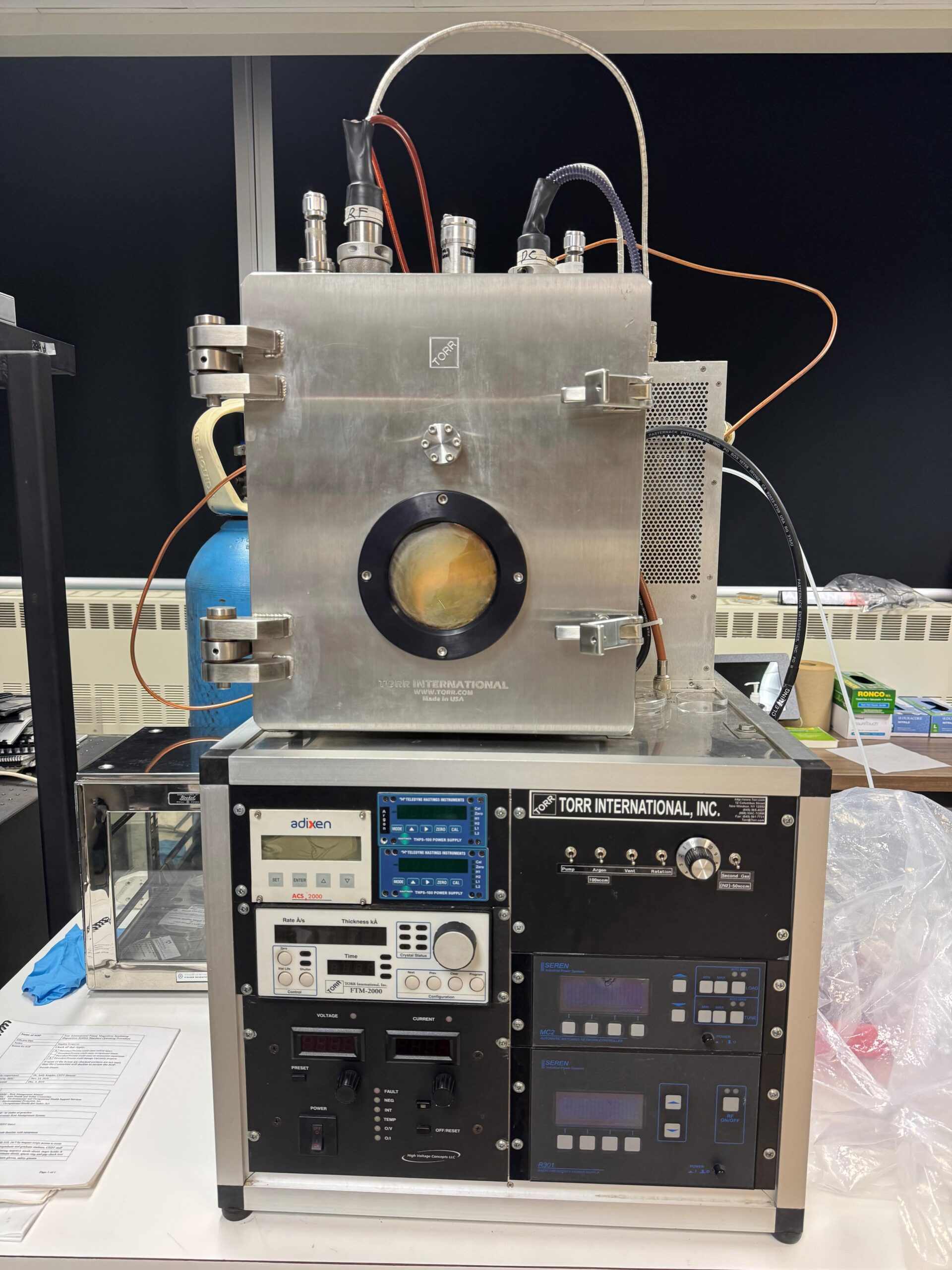 | Compact tabletop sputtering system designed for thin-film deposition. Features a DC/RF-compatible planar magnetron sputtering source and turbomolecular high-vacuum pumping. Location: JHE-317 Contact: Nebile Isik Goktas More details |
| Stylus Profilometer KLA-Tencor P7 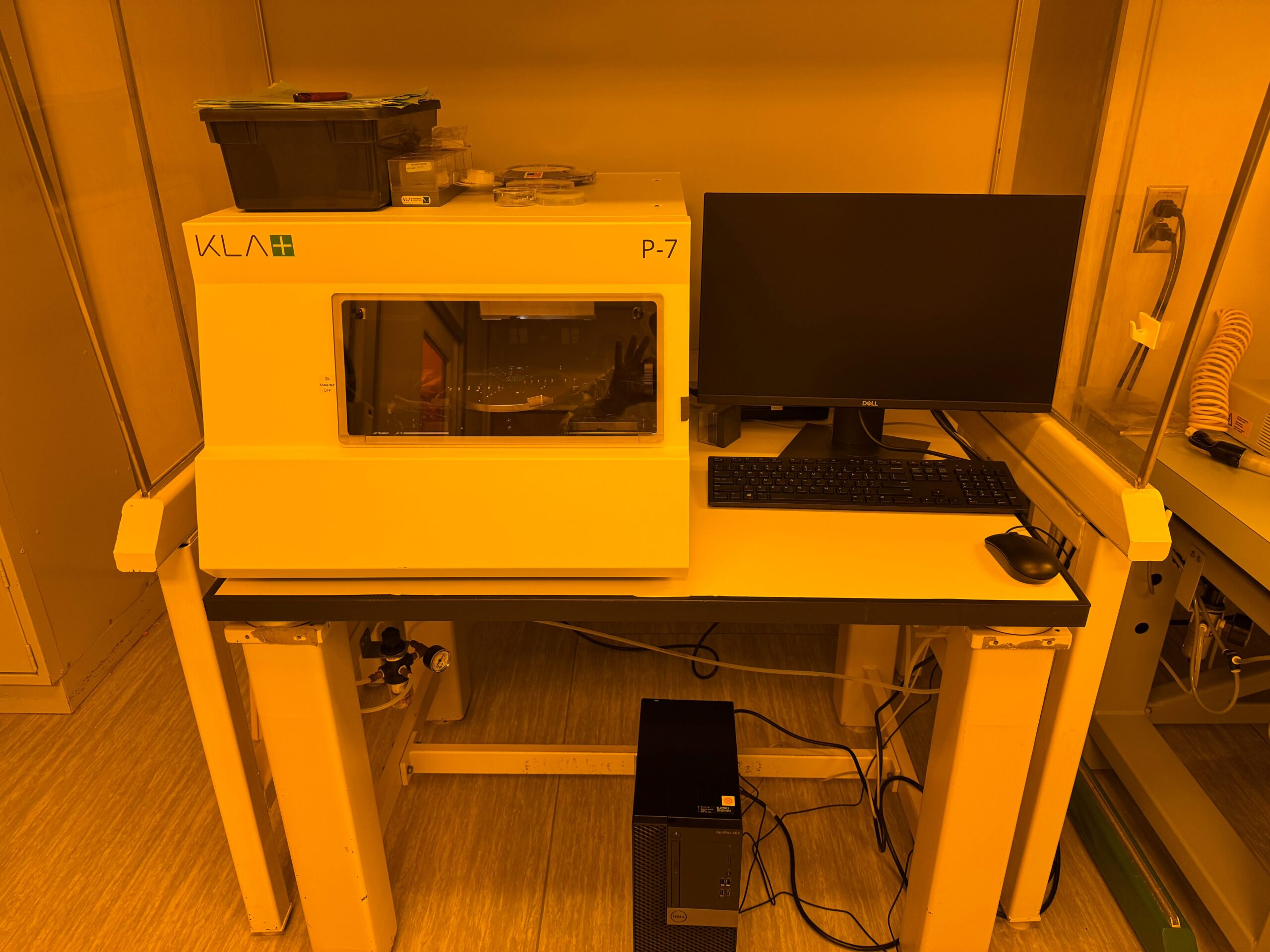 | Surface topography and film thickness measurement system utilizing a diamond stylus profiling mechanism. Supports programmable multi-location scanning, full-diameter unstitched measurements, and 2D or 3D characterization of step heights, surface roughness, wafer bow, and thin film stress. Location: JHE-A306 Contact: Nebile Isik Goktas More details |
| Thin Film Stress Measurement System KLA-Tencor FLX-2320  | Thin-film stress measurement system utilizing laser scanning to measure changes in the radius of curvature of a wafer induced by film deposition. Supports data analysis for calculating material properties, stress-temperature gradients, and stress relaxation behaviors with low measurement noise. Location: JHE-A306 Contact: Nebile Isik Goktas or Doris Stevanovic More details |
| Tube Furnace System Lindberg/Blue M STF55666 Series Moldatherm 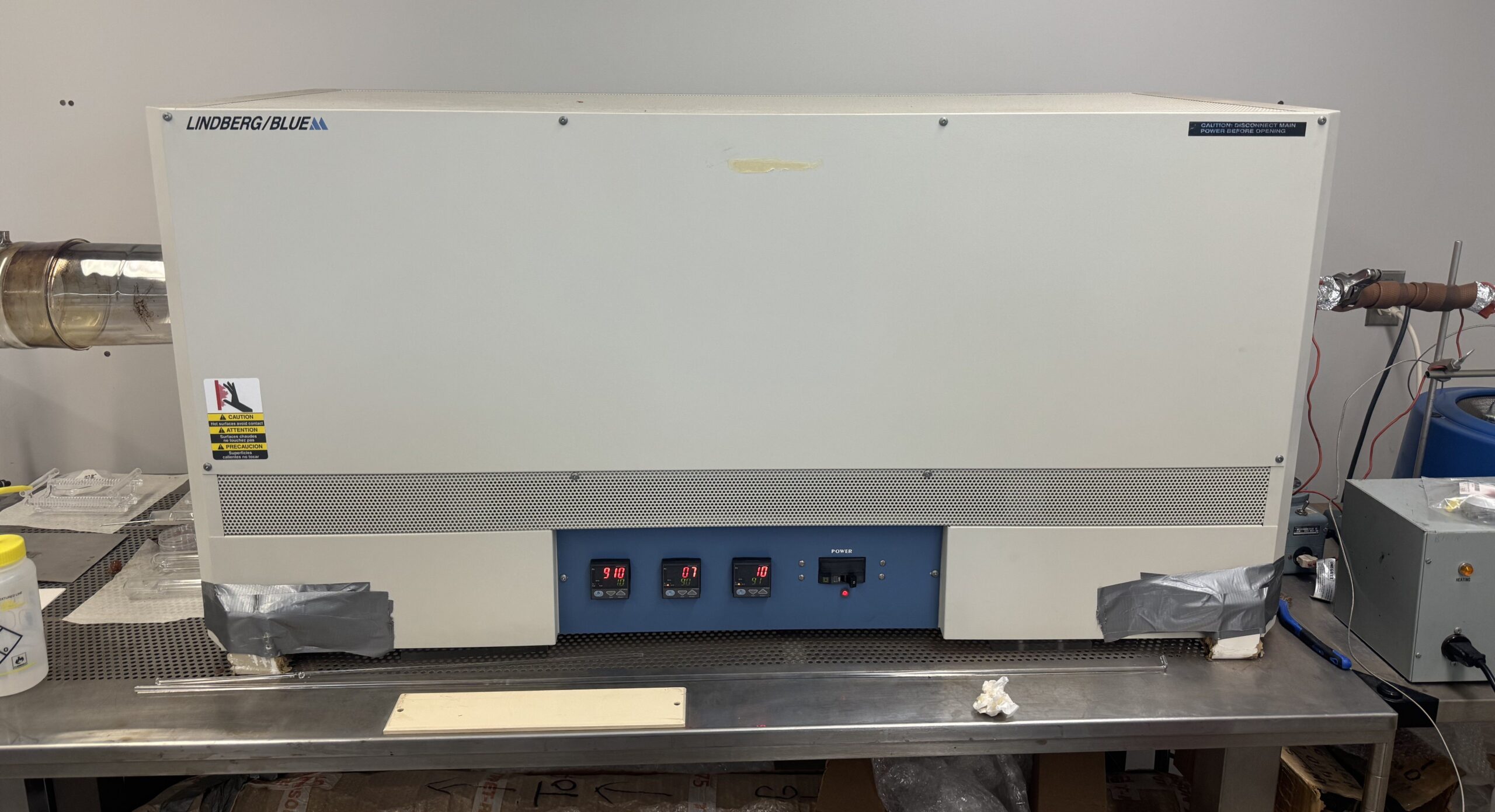 | Multi-zone tube furnace system designed for controlled thermal processing, annealing, and high-temperature material synthesis. Features double-shell insulated construction and independently programmable PID-controlled heating zones for stable thermal processing conditions. Location: TAB-205 Contact: Nebile Isik Goktas More details |
| UV Ozone Cleaner UV-2 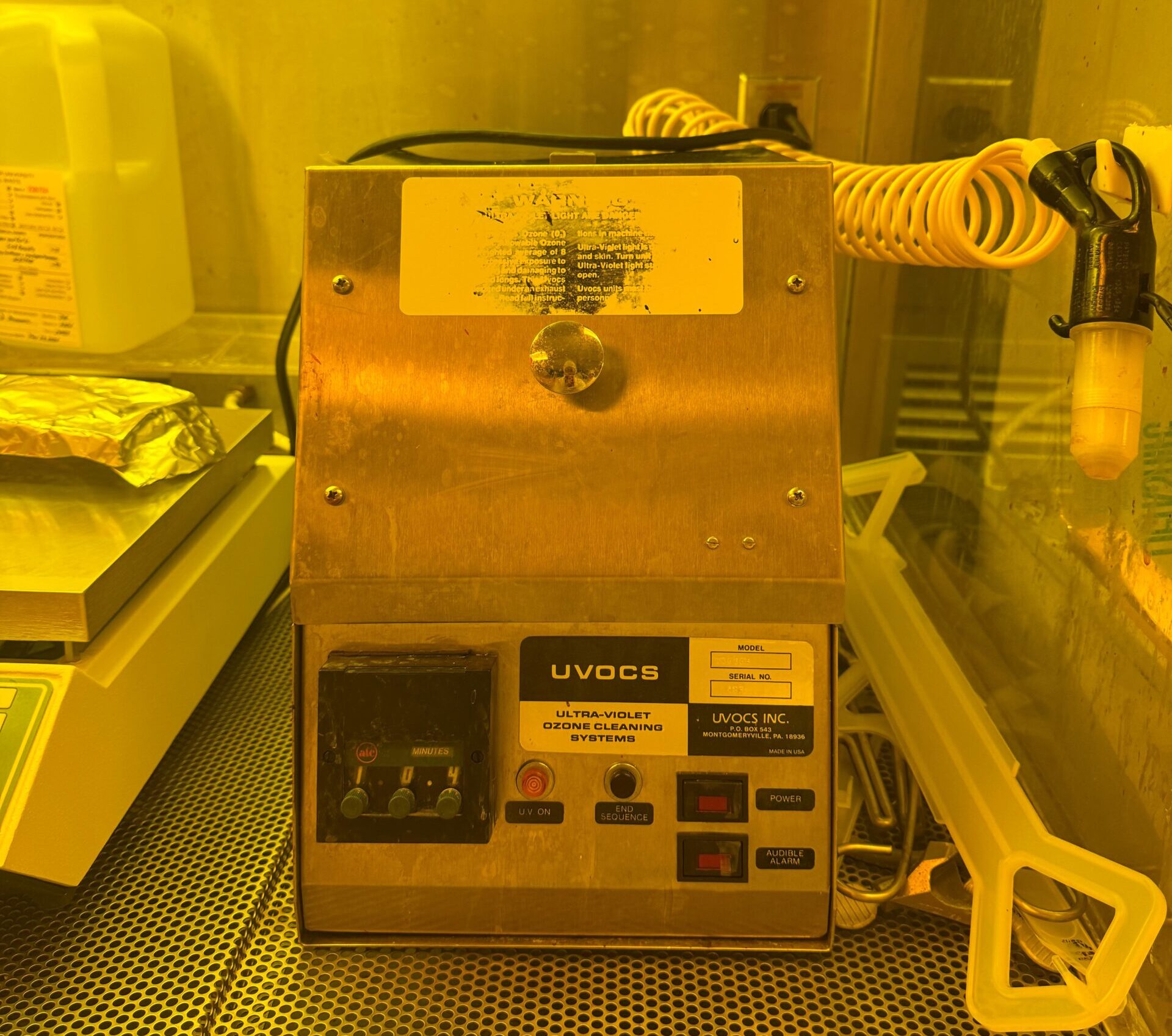 | Benchtop ultraviolet (UV) ozone cleaner designed for removing organic contaminants from substrates including silicon, gallium arsenide, sapphire, ceramics, and glass. Accommodates wafers up to a maximum size of 8″ and process temperatures up to 300°C. Location: JHE-A306 Contact: Nebile Isik Goktas or Doris Stevanovic Details |
| Water Purification System – Deionization MilliporeSigma Milli-DI 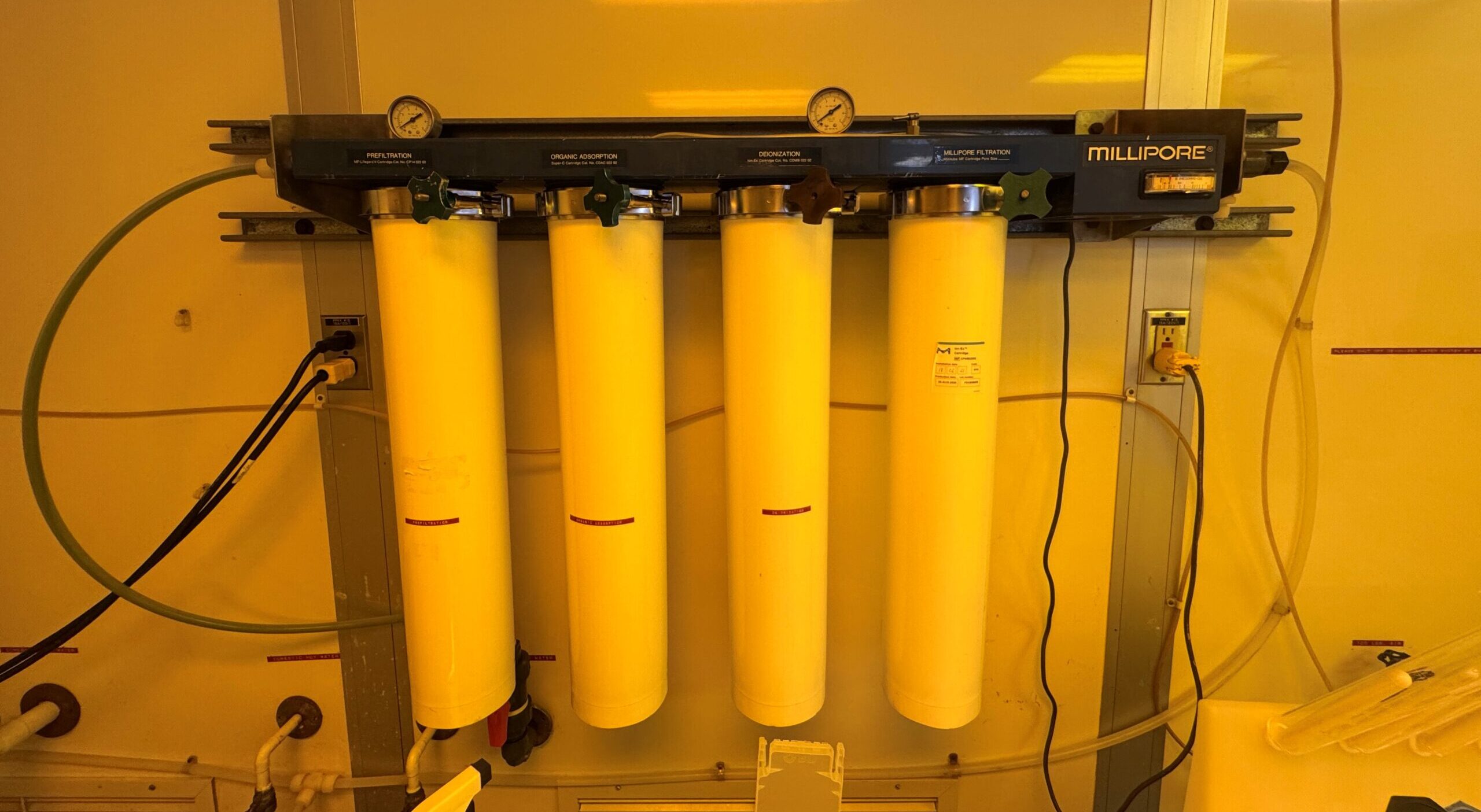 | Four-column water purification system configured to produce deionized (Type 2) water directly from a tap water feed source. The unit is battery-powered, eliminating the requirement for an electrical outlet connection. Location: JHE-A306 Contact: Doris Stevanovic More details |