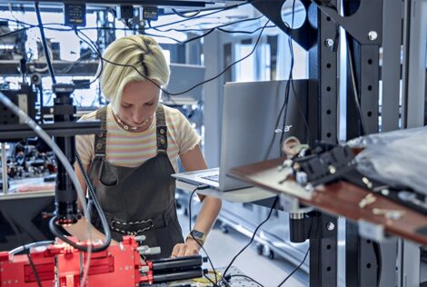
The Quantum Materials and Devices Group, headed by Dr. LaPierre, is focused on the development of semiconductor materials and devices at the quantum scale. Our current work focuses on the growth and characterization of semiconductors (Figure 1) and their application in quantum photonic and optoelectronic devices (Figure 2 and 3). Possible projects include:
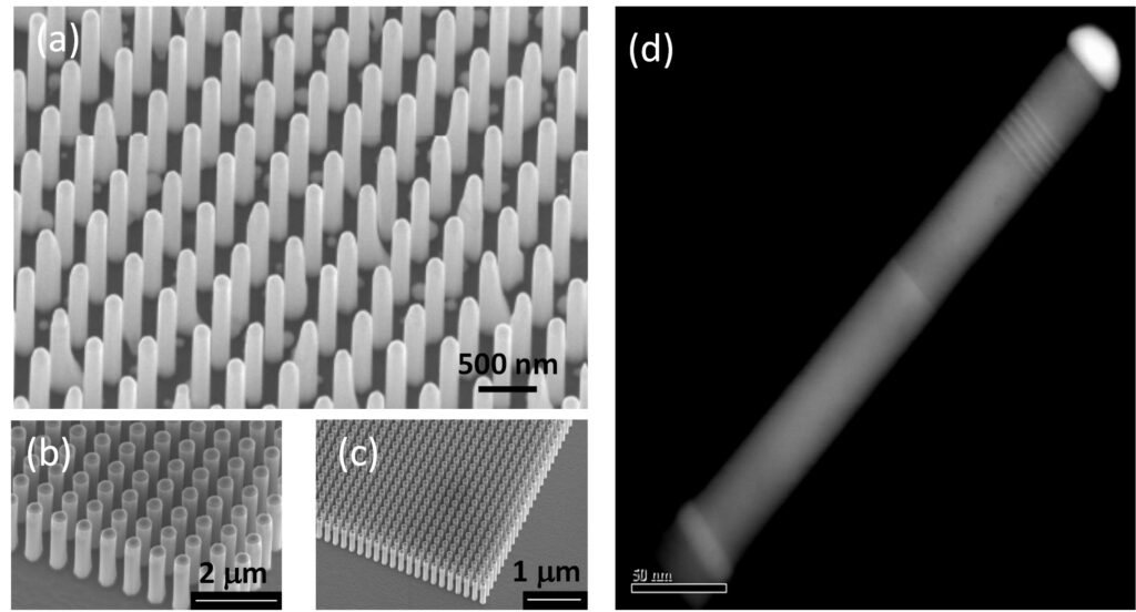
1. Quantum photonics: We design and create quantum metamaterials (Figure 2a-c) that display unique interactions with light (photons). For example, structures can be created that more efficiently absorb, reflect, or transmit light by manipulating photons. For example, the wavelength of light absorbed by a semiconductor nanostructure depends on its size, which has applications in advanced photovoltaics and photodetectors.
2.Quantum computing: We create quantum nanostructures for the creation or detection of single photons or entangled photon pairs. This work has applications in quantum computers, quantum communications, and quantum metrology. For example, semiconductor quantum dots (Figure 2d) can be implemented along the length of nanowires. These quantum dots are being used as single photon emitters.
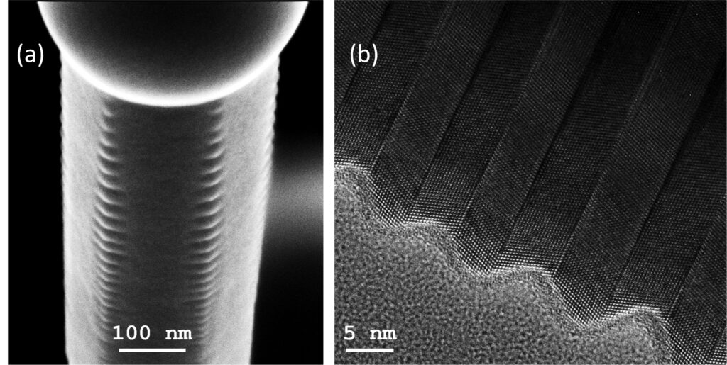
3.Energy devices: By creating “corrugated” nanowires (Figure 3), we can create a surface structure and internal crystal phases that control phonons (quantum unit of heat). This work has applications in thermoelectric devices that efficiently convert thermal energy into electrical power to be used for the harvesting of waste heat.
4. Nano + nuclear: Betavoltaics employ a radioactive isotope placed near a semiconductor. Beta particle emission (fast electrons) from the radioisotope results in electrical power generation from the semiconductor. Thus, betavoltaics operate in a manner similar to solar photovoltaics but replace photons with beta particles, generating electrical power by nuclear-to-electrical conversion. Betavoltaics have a wide variety of applications such as deep ocean monitoring, sensor networks, space satellites, etc. Using McMaster’s extensive nuclear engineering facilities, we are developing a novel approach to place radioisotopes in the space between nanostructures to improve the beta capture and betavoltaic device efficiency.
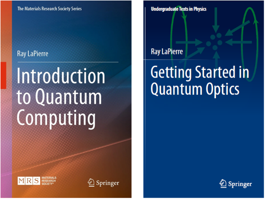
For more information, the following books by Dr. LaPierre may be useful:
We have a wide variety of experimental tools at McMaster:
Quantum Optics Lab:
Superconducting nanowire single photon detectors for single photon counting.
Micro-photoluminescence and Fourier transform infrared spectroscopy.
Centre for Emerging Device Technologies:
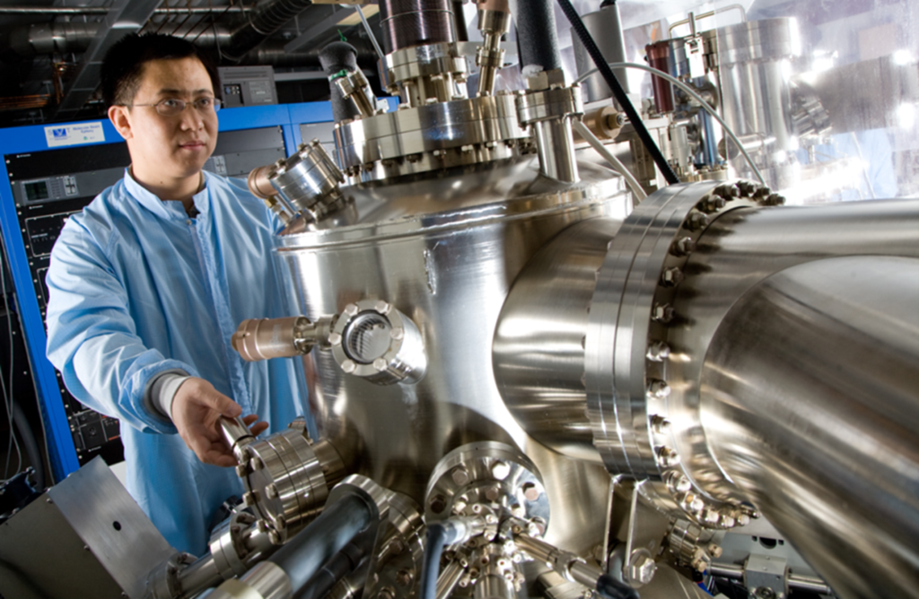
Molecular beam epitaxy (Figure 1) and metalorganic chemical vapour deposition system (MOCVD) for compound semiconductor deposition.
Cleanroom for device fabrication.
Canadian Centre for Electron Microscopy:
State-of-the-art electron beam characterization facility including scanning electron microscopy, high resolution transmission electron microscopy, energy dispersive x-ray spectroscopy, and electron energy loss spectroscopy. We also have focussed ion beam etching/deposition and atom probe tomography.
McMaster Analytical X-Ray Diffraction Facility:
A wide variety of x-ray diffraction equipment is available.
Figure 1. Molecular beam epitaxy system for semiconductor growth.Figure 2. (a-c). Scanning electron microscopy images of GaAs nanowire arrays. (d) Transmission electron microscopy image of a single GaP nanowire with GaAs quantum dots/wells. The Ga seed particle, responsible for nanowire growth, is visible as the bright hemisphere at the top (upper right) of the nanowire.Figure 3. (a) Scanning electron microscopy image of a single GaAs nanowire, showing surface faceting due to a twinning superlattice. (b) Transmission electron microscopy image of the superlattice twinning.
Each student is required to prepare/present a formal seminar, based upon extensive research work and literature surveys, in areas related to their current research. A pass/fail grade will be assessed based on overall performance in the course.
This course introduces group III-V semiconductor materials, heterostructures and devices including HBTs, HEMTs, laser diodes, photodiodes, and multi-junction solar cells.
An introductory course on nanoelectronics, quantum transport and mesoscopic physics including diffusive and ballistic transport in the classical and quantum regimes, quantum Hall effect, Coulomb blockade, quantum structures, superconductors, topological insulators, and quantum computing.
4 unit(s) Introductory statistics for engineering, error analysis of experimental data, data visualization and curve fitting, hypothesis testing and making decisions, ANOVA, sensors for engineering measurements, noise and interference, instrument response and uncertainty, reliability, and selected topics in state-of-the-art technologies.
Three lectures, one lab (three hours) every other week, one tutorial; second term
Prerequisite(s): Registration in Level III or above of any Engineering Physics program and ENGPHYS 2A04, ENGPHYS 2E04, ENGPHYS 2NE3, ENGPHYS 2QM3, and ENGPHYS 3W03.
3 unit(s) An introduction to quantum computing including qubits, entanglement, quantum key cryptography, teleportation, quantum circuits and algorithms, spin qubits.
3 unit(s) An introduction to quantum optics including single photon states, coherent states, standard quantum limit, Heisenberg limit, squeezed light, entanglement, and applications in metrology.
3 unit(s) An introduction to quantum computing including qubits, entanglement, quantum key cryptography, teleportation, quantum circuits and algorithms, spin qubits.