For the past few decades, Moore’s law which states that the number of devices on a chip will double every year, has been the driving force of the semiconductor industry. Yet, this miniturisation trend is now facing significant roadblocks as memory devices are reaching their scalability limit. To perpetuate this law, computer hardware has to be redesigned using neuromorphic materials that can mimic the human brain’s ability to perform cognitive tasks such as learning and pattern recognition. While computer algorithms can perform such tasks, their energy requirements is orders of magnituder higher than that of a human brain. Neuromorphic materials provide a means to obtain artificial synpases that can perform cognitive tasks with energy requirements that can rival that of the human brain.
Our research aims to develop highly-efficient smart materials for neuromorphic computing. We focus on ferroelectric materials, where a change in resistance can be induced by an external bias to mimic the change in synaptic weight occuring while our brain performs a cognitive task. Our research activities combine material synthesis (i.e. microwave-assisted hydrothermal synthesis, magnetron sputtering) with state-of-the-art characterisation techniques (aSNOM, AFM-IR, HAXPES), device fabrication and its subsequent performance analysis. We aim to understand the interplay between material nanostructure and device macroscopic properties to tune them to specific applications such as highly efficient artificial synpases, smart tactile sensors, or energy harvesting devices.
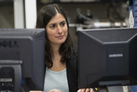
Gitanjali Kolhatkar is an Assistant Professor in Engineering Physics. She holds a BSc and an MSc in Physics from the University of Ottawa (2008 and 2010), and a PhD in Electrical Engineering from the University of Sherbrooke (2014). She conducted a postdoctoral fellowship at the Institut National de la Recherche Scientifique (2015-2019). In 2019, she was an invited professor at the Munich University of Applied Sciences, where she gave lectures in the Micro- and Nanotechnology graduate program, in addition to conducting research. From 2019-2022, she was an Alexander von Humboldt fellow at the University of Kiel, Germany. Her research interests and core expertise include structure–function relations in a variety of materials for applications in photovoltaics, memory devices, smart sensors, and artificial synapses.
Ph.D. , Electrical Engineering, University of Sherbrooke
M.Sc., Physics, University of Ottawa,
B.Sc., Physics, University of Ottawa
Alexander von Humboldt Post-doctoral research fellowship (2019-2022)
Honorary fellowship of Munich University of Applied Sciences (2019)
Kröger, E., Petraru, A., Hanff, A., Soni, R., Kalläne, M., Denlinger, J.D., Learmonth, T., Guo, J.-H., Smith, K.E., Schneller, T., Freelon, B., Kipp, L., Kohlstedt, H., Rossnagel, K., and Kolhatkar, G. (2022)
Mittermeier, B., Dörfler, A., Horoschenkoff, A., Katoch, R., Schindler, C., Ruediger, A.,and Kolhatkar, G. (2019)
Recent
Please refer to Google Scholar for an up-to-date list of all publications
Patents
Ruediger, A. Hadj Youssef, F. Ambriz-Vargas, G. Kolhatkar, M. A. Gauthier, R. Thomas, A. Sarkissian, U.S. Patent ref.: 773/14448.113 – “Ferroelectric Tunnel Junction and Method of Fabrication Thereof” (2017).
Journal Papers
E. Kröger, A. Petraru, A. Hanff, R. Soni, M. Kalläne, J.D. Denlinger, T. Learmonth, J.-H. Guo, K.E. Smith, T. Schneller, B. Freelon, L. Kipp, H. Kohlstedt, K. Rossnagel, G. Kolhatkar “Digging deeper: Buried layers and interfaces studied by modified total electron yield and soft X-ray absorption spectroscopy” Applied Physics Letters, 120 (18), 181601-1-6 (2022).
R. Marquardt, J. Cipo, F. Schlichting, G. Kolhatkar, H. Kohlstedt, H. Kersten “Correlation between properties of DC-magnetron sputtered thin niobium nitride films and plasma parameters” Thin Solid Films, 742, 139046 (2022).
A. Hadj Youssef, G. Kolhatkar, I. Amaechi, R. Katoch, Y. Gonzalez, A. Merlen, A. Ruediger “Giant step bunching on SrTiO3 thin films grown epitaxially on vicinal MgO (100) surfaces,” Applied Surface Science, 570, 151266 (2021).
J. Zhang, G. Kolhatkar, A. Ruediger “Localized surface plasmon resonance shift and its application in scanning near-field optical microscopy,” Journal of Materials Chemistry C, 9, 6960-6969 (2021).
A. Hadj Youssef, J. Zhang, A. Ehteshami, G. Kolhatkar, C. Dab, D. Berthomieu, A. Merlen, F. Légaré, A. Ruediger “Symmetry forbidden mode detection in SrTiO3 nanoislands with tip-enhanced Raman spectroscopy,” Journal of Materials Chemistry C, 125 (11), 6200-6208 (2021).
A. Lubio, A. Dörfler, J. Plathier, T. Dequivre, G. Kolhatkar, S. Charlebois, A. Ruediger “Correlation of local strain and temperature measurements in confocal Raman microscopy,” Journal of Raman Spectroscopy, 52(6), 1123 (2021).
I. Amaechi, A. Hadj Youssef, G. Kolhatkar, D. Rawach, C. Gomez-Yañez, J. Claverie, S. Sun, A. Ruediger“Ultrafast microwave-assisted hydrothermal synthesis and photocatalytic behaviour of ferroelectric Fe3+-doped BaTiO3 under simulated solar irradiation,” Catalysis Today, 360, 90 (2021) .
S. Sauze, M. R. Aziziyan, P. Brault, G. Kolhatkar, A. Ruediger, A. Korinek, D. Machon, R. Arès, A. Boucherif “Integration of 3D Nanographene into Mesoporous Germanium,” Nanoscale, 12 (47), 23984 (2020).
I. Amaechi, R. Katoch, G. Kolhatkar, S. Shuhui, A. Ruediger “Particle size effect on the photocatalytic kinetics of barium titanate powders,” Catalysis Science & Technology, 10 (18), 6274 (2020).
J. Zhang, A. Hadj Youssef, A. Dörfler, G. Kolhatkar, A. Merlen, A. Ruediger “Sample induced intensity variations of localized surface plasmon resonance in tip-enhanced Raman spectroscopy,” Optics Express, 28 (18), 25998 (2020).
E. Sokullu, M. Pinsard, J. Zhang, J. Plathier, G. Kolhatkar, A. Blum, F. Légaré, A. Ruediger, T. Ozaki, M. A. Gauthier “Plasmonic enhancement of two-photon excitation fluorescence by colloidal assemblies of very small AuNPs templated on M13 phage,” Biomacromolecules, 21 (7), 2705 (2020).
A. Hadj Youssef, J. Zhang, A. Dörfler, G. Kolhatkar, A. Merlen, A. Ruediger “Topography-induced variations of localized surface plasmon resonance in tip-enhanced Raman configuration,” Optics Express, 28 (9), 14161 (2020).
T. Dugger, S. Sarkar, S. Correa-Garhwal, M. Zhernenkov, Y. Zhang, G. Kolhatkar, R. Mohan, L. Cruz, A. Lubio, A. Ruediger, C. Hayashi, K. Uhrich, D. Kisailus, (2020) “Ultrastructure and Mechanics of Annealed Nephila clavipes Major Ampullate Silk,” Biomacromolecules, 21(3), 1186.
A. Dörfler, G. Kolhatkar, U. Wagner, A. Ruediger “The Effects of Thin Film Homogeneity on the Performance of Ferroelectric Tunnel Junctions,” Journal of Physics: Condensed Matter, 32, 185302 (2020).
C. Parisien, G. Kolhatkar, A. Dörfler, F. Crispino, A. Lajeunesse, A. Ruediger “Contrast enhancement for the recovery of obliterated serial numbers in different polymers by correlated Raman imaging of strain, phonon-lifetime and strain-induced anisotropy,” Analytical Chemistry, 91(22), 14247 (2019).
B. Mittermeier, A. Dörfler, A. Horoschenkoff, R. Katoch, C. Schindler, A. Ruediger, G. Kolhatkar, “CMOS compatible Hf0.5Zr0.5O2 ferroelectric tunnel junctions for neuromorphic devices,” Advanced Intelligent Systems, 1(5), 1900034 (2019).
I. Amaechi, G. Kolhatkar, D. Rawach, S. Sun, A. Ruediger “B-site modified photoferroic Cr3+-doped barium titanate nanoparticles: microwave-assisted hydrothermal synthesis, photocatalytic and electrochemical properties,” RSC Advances, 9, 20806 (2019).
G. Kolhatkar, M. Nicklaus, A. Hadj Youssef, C. Cojocaru, M. Rivard, A. Merlen, F. Légaré, A. Ruediger, “Second harmonic generation investigation of symmetry breaking and flexoelectricity induced by nanoindentations in SrTiO3,” Advanced Functional Materials, 29 (36) 1901266 (2019).
G. Kolhatkar, C. Parisien, A. Ruediger, C. Muehlethaler “Latent fingermark imaging by single-metal deposition of gold nanoparticles and surface enhanced Raman spectroscopy,” Frontiers in Chemistry, 7, 440 (2019).
G. Kolhatkar, B. Mittermeier, Y. Gonzalez, F. Ambriz-Vargas, M. Weismueller, A. Sarkissian, C. Gomez-Yanez, R. Thomas, C. Schindler, A. Ruediger, “BiFe1‑xCrxO3 ferroelectric tunnel junctions for neuromorphic systems”, ACS Applied Electronic Materials, 1 (6), 828 (2019) .
M. Kracklauer, F. Ambriz-Vargas, G. Kolhatkar, B. Huber, C. Schindler, A. Ruediger, “Oxygen vacancy filament-based resistive switching in Hf0.5Zr0.5O2 thin films for non-volatile memory,” Advanced Materials Letters, 10 (6), 405 (2019).
M. Nicklaus, G. Kolhatkar, J. Plathier, C. Dab, A. Ruediger, “Direct observation of core-shell structures in individual lead titanate ferroelectric nanostructures by tip-enhanced refractive index mapping,” Advanced Functional Materials, 29 (2), 1806770 (2018).
M. Agati, S. Boninelli, P. Castrucci, G. Amiard, R. Pandiyan, G. Kolhatkar, R. Dolbec, A. Ruediger, M. A. El Khakani, My Ali, “Formation of silicon nanocrystal chains induced via Rayleigh instability in Si/SiO2 core/shell ultrathin nanowires synthesized by an inductively-coupled-plasma torch process,” Journal of Physics: Materials, 2.1 (2018): 015001(2018).
A. Hadj-Youssef, G. Kolhatkar, A. Merlen, R. Thomas, A. Ruediger, “Surface Preparation and the Evolution of Atomically Flat Step Terrace Morphology of MgO Single Crystals,” AIP Advances, 8, 095025 (2018).
M. Barberio, S. Vallière, M. Sciscio, G. Kolhatkar, A. Ruediger, and P. Antici, “Graphitization of Diamond by Laser-Accelerated Proton Beams,” Carbon, 139, 531-537 (2018).
G. Kolhatkar, A. Merlen, J. Zhang, C. Dab, G. Q. Wallace, F. Lagugné-Labarthet, A. Ruediger, “Optical near-field mapping of plasmonic nanostructures prepared by nanosphere lithography,”Beilstein Journal of Nanotechnology, 9, 1536-1543(2018).
G. Kolhatkar, F. Ambriz-Vargas, B. Huber, R. Thomas, A. Ruediger, “Thermionic Emission Based Resistive Memory with Ultrathin Ferroelectric BiFe1−xCrxO3 Films Deposited by Mineralizer-Free Microwave-Assisted Hydrothermal Synthesis,” Crystal Growth & Design, 18 (3), 1864-1872(2018).
G. Kolhatkar, A. Boucherif, A.R. Boucherif, A. Dupuy, L. G. Frechette, R. Ares, A. Ruediger, “Extreme temperature stability of thermally insulating graphene-mesoporous-silicon nanocomposite,” Nanotechnology, 29, 145701 (2018).
G. Kolhatkar, J. Plathier, A. Ruediger, “Nanoscale investigation of materials, chemical reactions, and biological systems by tip enhanced Raman spectroscopy – A review,” Journal of Materials Chemistry C, 6, 1307-1319 (2018) .
C. Dab, G. Kolhatkar, J. Plathier, R. Thomas, A. Ruediger, “Dependence of Apertureless Scanning Near-Field Spectroscopy on Nanoscale Refractive Index Changes,” Plasmonics, 13 (1), 99-106 (2018).
C. Parisien, G. Kolhatkar, F. Crispino, A. Lajeunesse, A. Ruediger, “Reconstruction of obliterated characters in polycarbonate through spectral imaging,” Analytical Chemistry, 89 (21), 11648-11652 (2017).
G. Kolhatkar, F. Ambriz-Vargas, R. Thomas, A. Ruediger, “Microwave-assisted hydrothermal synthesis of BiFexCr1-xO3 ferroelectric thin films,” Crystal Growth & Design, 17 (11), 5697-5703 (2017).
G. Kolhatkar, J. Plathier, A. Pignolet, A. Ruediger, “Effect of the Gold Crystallinity on the Enhanced Luminescence Signal of Scanning Probe Tips in Apertureless Near-Field Optical Microscopy,” Optics Express, 25 (21), 25929-25937 (2017).
T. Dequivre, G. Kolhatkar, A. Hadj-Youssef, X.T. Le, G.M. Brisard, A. Ruediger, S.A. Charlebois “Wet Metallization of High Aspect Ratio TSV Using Electrografted Polymer Insulator to Suppress Residual Stress in Silicon,” IEEE Transactions on Device and Materials Reliability, 17 (3), 514-521 (2017).
F. Ambriz-Vargas, G. Kolhatkar, M. Broyer, A. Hadj-Youssef, R. Nouar, A. Sarkissian, R. Thomas, C. Gomez-Yáñez, M. A. Gauthier, A. Ruediger, “A Complementary Metal Oxide Semiconductor Process-Compatible Ferroelectric Tunnel Junction,” ACS Appl. Mater. Interfaces, 9 (15), 13262-13268 (2017).
F. Ambriz-Vargas, G. Kolhatkar, R. Thomas, R. Nouar, A. Sarkissian, C. Gomez-Yanez, M. A. Gauthier, A. Ruediger, “Tunneling electroresistance effect in a Pt/Hf0.5Zr0.5O2/Pt structure,” Appl. Phys. Lett., 110, 93106 (2017).
R. Boucherif, A. Boucherif, G. Kolhatkar, A. Ruediger, R. Arès, “Graphene-Mesoporous Si Nanocomposite as a Compliant Substrate for Heteroepitaxy,” Small, 13, 1603269 (2017).
I. Velasco-Davalos, F. Ambriz-Vargas, G. Kolhatkar, R. Thomas, A. Ruediger, “Synthesis of BiFeO3 thin films on single-terminated Nb:SrTiO3 (111) substrates by intermittent microwave assisted hydrothermal method”, AIP Advances, 6, 065117 (2016) .
G. Kolhatkar, A. Boucherif, C. Dab, S. Fafard, V. Aimez, R. Ares, A. Ruediger, “Composition Variation in Al-Based Dilute Nitride Alloys Using Apertureless Scanning Near-Field Optical Microscopy”, Phys. Chem. Chem. Phys., 18, 30546-30553 (2016).
G. Kolhatkar, A.Boucherif, Y. A. Bioud, S. Fafard, A. Ruediger, V. Aimez, R. Arès, “Electrical and structural properties of AlGaNAs alloys grown by chemical beam epitaxy,” Physica Status Solidi (B),253 (5), 918-922 (2016).
R. Cheriton, M. M. Wilkins, P. Sharma, C. E. Valdivia, A. H. Trojnar, H. Schriemer, J. Gupta, B. Bouzazi, G. Kolhatkar, et al., “Design Optimizations of InGaAsN(Sb) subcells for Concentrator Photovoltaic Systems,” Journal of Vacuum Science and Technology B, 34 (2), 02M103-1-5 (2015).
G. Kolhatkar, A. Boucherif, C.E. Valdivia, S.G. Wallace, S. Fafard, V. Aimez, R. Arès, “Growth optimization and optical properties of AlGaNAs alloys,” Journal of Applied Physics, 115, 163513 (2014).
G. Kolhatkar, A. Boucherif, C.E. Valdivia, S.G. Wallace, S. Fafard, V. Aimez, R. Arès, “Al-enhanced N incorporation in GaNAs alloys grown by Chemical Beam Epitaxy,” Journal of Crystal Growth, 380, 256-260 (2013).
B. Paquette, M. DeVita, A. Turala, G. Kolhatkar, A. Boucherif, A. Jaouad, et al., “Optimization of p-doping in AlGaAs grown by CBE using TMA for AlGaAs/GaAs tunnel junctions,” Journal of Crystal Growth, 374, 1-4 (2013).
G.Kolhatkar, J.F. Wheeldon, C.E. Valdivia, A.W. Walker, S. Fafard, A. Turala, et al., “Current–voltage measurements within the negative differential resistance region of AlGaAs/AlGaAs tunnel junctions for high concentration photovoltaics,” International Journal of Nanoscience, 11, 1240014 (2012).
J.F. Wheeldon, C. E. Valdivia, A. Walker, G. Kolhatkar, A. Jaouad, et al., “Performance Comparison of AlGaAs, GaAs and InGaP Tunnel Junctions for Concentrated Multi-Junction Solar Cells,” Progress in Photovoltaics: Research and Applications, 19 (4), 442-452(2010).
4 unit(s) Electronic properties of semiconductors: non-equilibrium carrier conditions; steady state and non-steady state; p-n junctions; Schottky diodes; bipolar junction transistors. Detailed coverage of a range of diodes including photodiodes, solar cells, light emitting diodes, zener diodes, and avalanche diodes.
Three lectures, one tutorial, one lab (three hours) every other week; winter term
Prerequisite(s): Credit in at least one of the following: ELECENG 2EI4, ENGPHYS 3BA3, 3BA4, MATLS 2Q03 or Credit or Registration in at least one of the following: ENGPHYS 3SM3, PHYSICS 3K03
4 unit(s) Detailed description of fabrication technologies used in the semiconductor industry; computer modelling of device fabrication process and device performance; device fabrication in a cleanroom environment.
Three lectures, one lab (three hours); first term
Prerequisite(s): One of ENGPHYS 3PN4, ENGPHYS 3SM3, or MATLS 3Q03
4 unit(s) Detailed description of fabrication technologies used in the semiconductor industry; computer modelling of device fabrication process and device performance; device fabrication in a cleanroom environment.